Capacitive electrode having semiconductor layers with an interface of separated grain boundaries

a technology of capacitance and semiconductor layers, applied in the field of capacitance electrodes, can solve the problems of capacitor capacitance drop, electrical conductivity damage, bad effect produced on electrical conductivity, etc., and achieve the effect of reducing leakage current, reducing crystallization temperature, and reducing leakage curren

Inactive Publication Date: 2006-02-09
RENESAS ELECTRONICS CORP
View PDF8 Cites 2 Cited by
  • Summary
  • Abstract
  • Description
  • Claims
  • Application Information

AI Technical Summary

Benefits of technology

[0017] As is evident from FIGS. 10, 11 and 12, a tantalum pentoxide film has a small leakage current but has a high crystallization temperature. Contrarily, a niobium pentoxide film has a low crystallization temperature but has a large leakage current. On the basis of the results, the inventors have considered that a layered film of a tantalum pentoxide film and a niobium pentoxide film is effective. Specifically, a niobium pentoxide film is formed on a bottom electrode, and the resultant is heat-treated at a temperature lower than 750° C. so as to be crystallized. A tantalum pentoxide film is formed thereon, and the resultant is heat-treated. In this way, tantalum pentoxide is laminated on the undercoat having a crystal structure of niobium pentoxide. As a result, the crystallization temperature of the tantalum pentoxide film is affected by the crystal structure of the niobium pentoxide film so as to be made low. Simultaneously, the tantalum pentoxide film is present in the layered film; therefore, the leakage current density can also be kept small.
[0034] By making the capacitor dielectric film into a layered film and separating crystal boundaries in the dielectric film, leakage current can be decreased. Furthermore, by making the film thickness of the insulator film constituting the layered film small, stress in the film is reduced and the density of the film and the morphology thereof are improved so that leakage current can be decreased.

Problems solved by technology

If the plug reacts with the bottom electrode, a bad effect is produced on electrical conductivity.
The problem of the drop in the capacitor capacitance is also generated in the case of forming a silicon nitride film on the surface of the bottom electrode to prevent oxidation of silicon.
As a result, the electrical conductivity thereof is damaged.
Even if the oxidation temperature in the heat treatment is made low so that the oxidation of the bottom electrode and the barrier metal can be suppressed, the problems are not fundamentally solved if the crystallization temperature cannot be made low.
As far as tantalum pentoxide is used as the capacitor dielectric film, it is very difficult to make the temperature for crystallizing tantalum pentoxide as low as 750° C. or less.
As understood from FIG. 12, however, the inventors found out a problem that when niobium pentoxide is added, leakage current density increases.

Method used


Image

  • Capacitive electrode having semiconductor layers with an interface of separated grain boundaries
  • Capacitive electrode having semiconductor layers with an interface of separated grain boundaries
  • Capacitive electrode having semiconductor layers with an interface of separated grain boundaries

Examples


embodiment 1

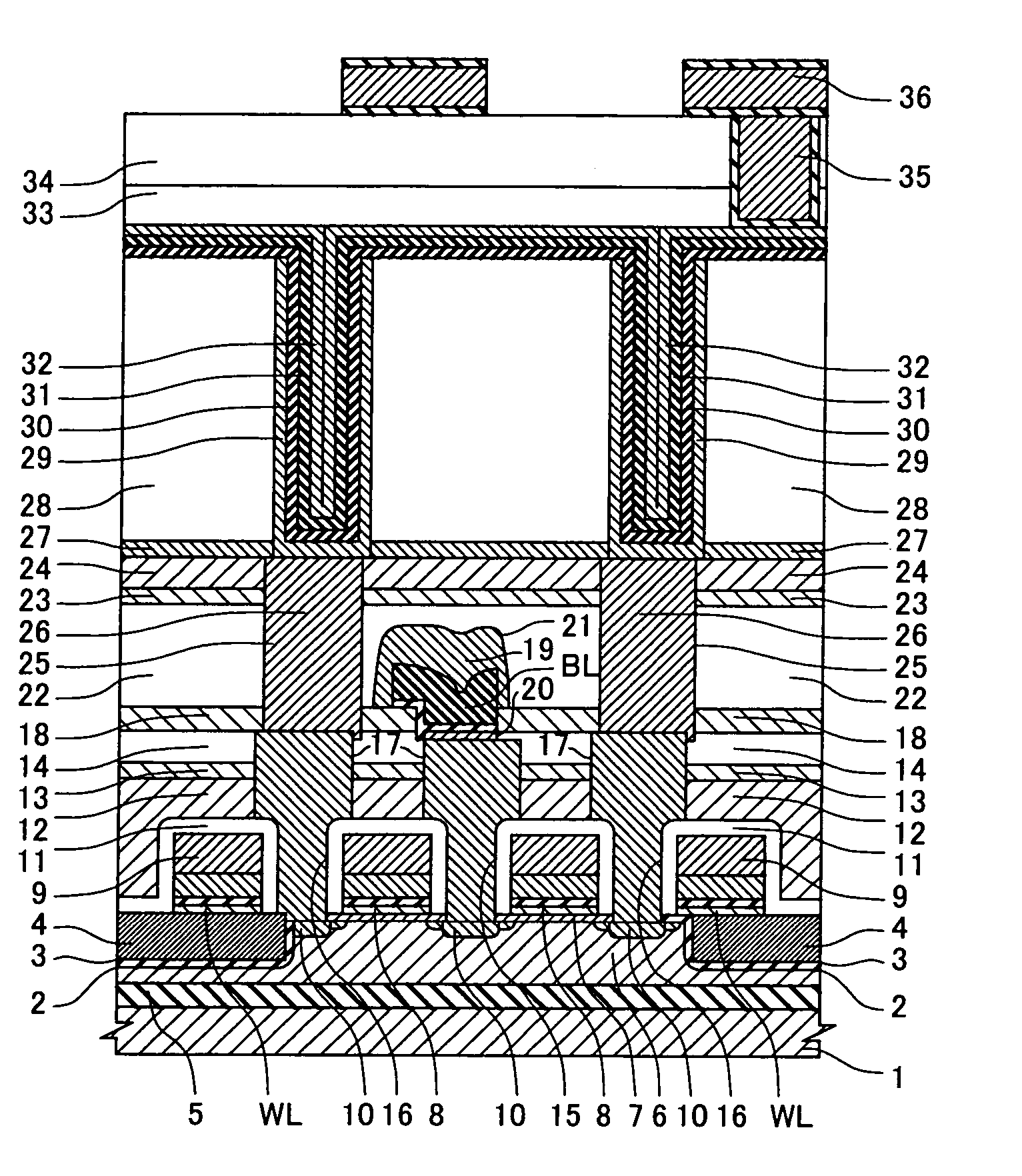
[0051] Referring-to FIG. 1, Embodiment 1 of the present invention will be described. This is an embodiment wherein the present invention is applied to a semiconductor memory device having a MIM capacitor using a dielectric film made of a layered film composed of a niobium pentoxide film and a tantalum pentoxide film, in particular, such a DRAM.

[0052] A process for producing the DRAW will be described.

[0053]FIG. 1 is a sectional view of the DRAW to which a capacitor of the present invention is applied. First, an element isolation region and a p-type well 6 to which an impurity is introduced are formed in a semiconductor substrate 1. For a P-type, a semiconductor substrate 1 made of single crystal silicon having a resistivity of 10 Ωcm is prepared. On the semiconductor substrate 1 are deposited, for example, a thin silicon oxide (not illustrated) having a film thickness of about 10 nm and formed by wet oxidation at about 850° C. and a silicon nitride film (not illustrated) having a ...

embodiment 2

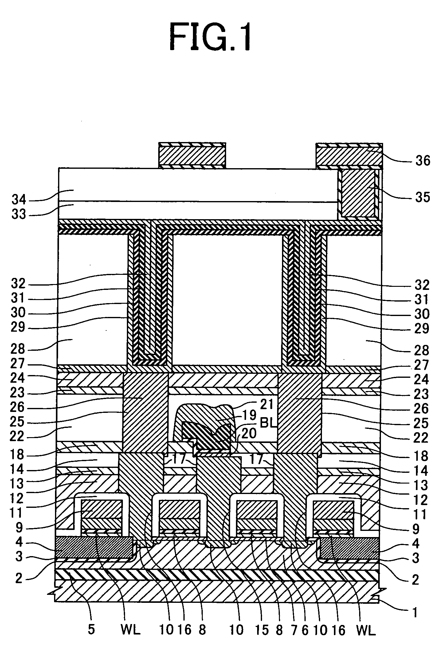
[0095] Embodiment 2 of the present invention will be described, referring to FIG. 2. This is an embodiment wherein an MIS capacitor using a dielectric film made of a layered film composed of a niobium pentoxide film and a tantalum pentoxide film is applied to a semiconductor memory device, in particular, such a DRAM.

[0096] The DRAM of the present embodiment is the same as in Embodiment 1 except differences in data-storing capacitor element structure. Accordingly, only the differences will be described hereinafter, and description on the same matters is omitted.

[0097] The process for producing the DRAM of Embodiment 2 is the same as in Embodiment 1 about the steps before the plug 26 is formed inside the through hole 25. In Embodiment 2, the plug 26 is formed by depositing a polycrystalline silicon film doped with an N-type impurity (such as P (phosphorus)) by CVD and then etching-back this polycrystalline silicon film so as to cause some parts thereof to remain inside the through h...

embodiment 3

[0109]FIG. 3 is a sectional view of a MISFET which is a semiconductor device of Embodiment 3. This is an example wherein a dielectric film made of a layered film composed of a niobium pentoxide film and a tantalum pentoxide film is used as a gate insulator film of the MISFET.

[0110] First, a semiconductor substrate 101, which is the same as the semiconductor substrate 1 in Embodiment 1, is prepared, and a groove 102 of an isolation element region is made in a main face of the semiconductor substrate 101 and a silicon oxide film 103 is formed inside the groove 102. The formation of the groove 102 and the silicon oxide film 103 is performed in the same way as the formation of the groove 2 and the silicon oxide film 4 in Embodiment 1.

[0111] Next, niobium pentoxide is deposited on the whole surface of the semiconductor substrate 101, and then crystallized to form a niobium pentoxide film 104. Furthermore, a tantalum pentoxide film is deposited on the niobium pentoxide film 104, and cry...


PUM

PropertyMeasurementUnit
thicknessaaaaaaaaaa
temperatureaaaaaaaaaa
pressureaaaaaaaaaa

Abstract

The present invention relates to a structure of a capacitor, in particular using niobium pentoxide, of a semiconductor capacitor memory device. Since niobium pentoxide has a low crystallization temperature of 600° C. or less, niobium pentoxide can suppress the oxidation of a bottom electrode and a barrier metal by heat treatment. However, according to heat treatment at low temperature, carbon incorporated from CVD sources into the film is not easily oxidized or removed. Therefore, a problem that leakage current increases arises. As an insulator film of a capacitor, a layered film composed of a niobium pentoxide film and a tantalum pentoxide film, or a layered film composed of niobium pentoxide films is used. By the use of the niobium pentoxide film, the dielectric constant of the capacitor can be made high and the crystallization temperature can be made low. By multiple-stage formation of the dielectric film, leakage current can be decreased.

Description

BACKGROUND OF THE INVENTION [0001] 1. Field of the Invention [0002] The present invention relates to a technique suitable for a semiconductor device and a process for producing the same, in particular, a semiconductor device having a capacitor, for example, a dynamic random access memory (DRAM), and a process for producing the same. [0003] 2. Description of Related Art [0004] It is known that for large scale integration of semiconductor devices or other purposes, a tantalum pentoxide film having a dielectric constant of several tens is adopted instead of a silicon oxide film (dielectric constant: about 4) or a silicon nitride film (dielectric constant: about 7), which has been conventionally used as a capacitor dielectric film (for example, JP-A No. 139288 / 1998). [0005] As a process for producing a capacitor having the tantalum pentoxide dielectric film, there is known a process of forming a tantalum pentoxide film on a capacitor bottom electrode, heat-treating the film to be crysta...

Claims


Application Information

Patent Timeline
Patent Type & Authority Applications(United States)
IPC IPC(8): H01L29/94C23C16/18H01L27/04C23C16/40C23C16/44C23C16/56H01L21/02H01L21/314H01L21/316H01L21/822H01L21/8234H01L21/8242H01L27/06H01L27/108H01L29/78
CPCC23C16/18H01L28/90C23C16/56H01L21/02175H01L21/02183H01L21/02194H01L21/022H01L21/02271H01L21/02356H01L21/31604H01L21/31637H01L27/10814H01L27/10852H01L27/10882H01L27/10894H01L28/40H01L28/56H01L28/75C23C16/405H10B12/315H10B12/033H10B12/48H10B12/09
Inventor MATSUI, YUICHIHIRATANI, MASAHIKO
Owner RENESAS ELECTRONICS CORP
Why Eureka
Try Eureka