Sapphire substrate, epitaxial substrate and semiconductor device

Inactive Publication Date: 2006-03-02
KYOCERA CORP
View PDF3 Cites 59 Cited by
  • Summary
  • Abstract
  • Description
  • Claims
  • Application Information

AI Technical Summary

Benefits of technology

[0042] With this constitution, a high efficiency light emitting device can be manufactured stably, with the surface smoothed without being affected by the variations in the light emitting device structure. It is also made possible to reduce the time required for growing

Problems solved by technology

The active layer 106 is typically formed in quantum well structure as described above, which results in a change in energy band structure due to the strong piezoelectric field, leading to a problem with respect to improvement of characteristics.
However, in the nitride semiconductors that are used at present, a decrease in the threshold current of the laser can hardly be achieved by intentionally generating a strain.
This is because the crystal has C axis orientation with respect to the direction of growth of the nitride semiconductor, and therefore the energy band structure does not change effectively.
In the case of a light emitting diode, too, the piezoelectric field generated in the active layer decreases the probability of carrier recombination, thus hindering the improvement of luminance.
However, as the enhancement type FET made of nitride semiconductor is not available at present and there are many restrictions on the design of circuit placing limitations on the applications thereof, there has been a strong demand for the enhancement type FET made of nitride semiconductor.
While the design of a circuit may require the depression type FET, which needs two power supplies of positive and negate voltages in order to operate, it results in such problems as increased power consumption and larger number of components in the circuit that uses it.
Among these, the latter is not practical since it is difficult to obtain large 4H—SiC (11-20) substrate with the current manufacturing techniques and the method is not suited for volume production.
Through researches conducted by the inventors of the present application and others, it has been found that growing the nitride semiconductor on R-plane sapphire substrate has such problems that much threading dislocations and stacking faults are introduced into the crystal due to a large difference in the lattice constant and non-polarity of sapphire, and that unfavorable form of crystal is involved that makes it difficult to form a steep interface that is required to manufacture the semiconductor device.
Although the method described in Applied Physics Letters, Vol. 84 (2004), pp 3663-3665 is useful in that consideration is given to the piezoelectric field in the active layer 127, it is not suited for practical applications because o

Method used


Image

  • Sapphire substrate, epitaxial substrate and semiconductor device
  • Sapphire substrate, epitaxial substrate and semiconductor device
  • Sapphire substrate, epitaxial substrate and semiconductor device

Examples


first embodiment

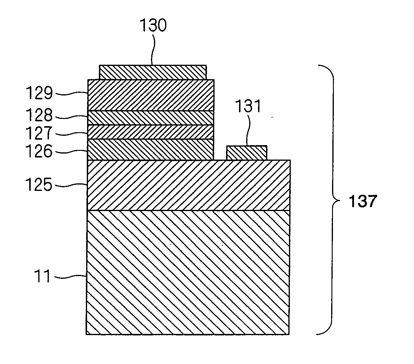
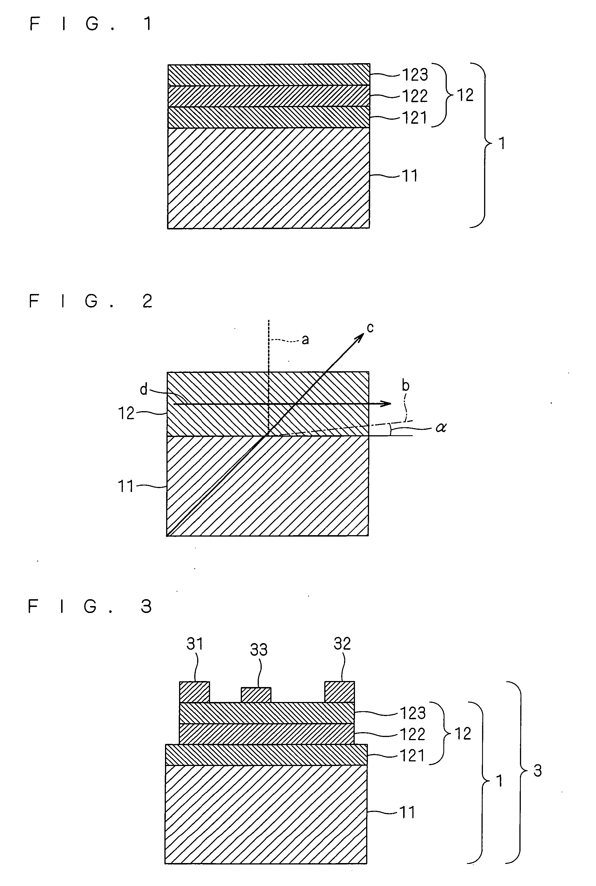
[0064]FIG. 1 is a schematic sectional view showing an epitaxial substrate according to this embodiment. As shown in FIG. 1, the epitaxial substrate 1 has a stacked layers structure 12 comprising a base layer 121, a channel layer 122 and a barrier layer 123 formed successively on one of the principal surfaces of a semiconductor growing substrate 11 made of sapphire. The base layer 121 is formed from aluminum gallium nitride where molar ratio x of AlN is in a range of 0.5≦x≦1.0. The channel layer 122 is formed from GaN or GaInN. The barrier layer 123 is formed from AlGaN.

[0065] The stacked layers structure 12 made of nitride semiconductor is formed so that [0001] axis (denoted as d in FIG. 2, hereinafter referred to as C axis) is oriented parallel to the principal plane of the semiconductor growing substrate 11.

[0066] As shown in FIG. 2, the angle between one principal plane of the semiconductor growing substrate 11 and (01-12) plane of sapphire (denoted as “b” in FIG. 2) is the off...

second embodiment

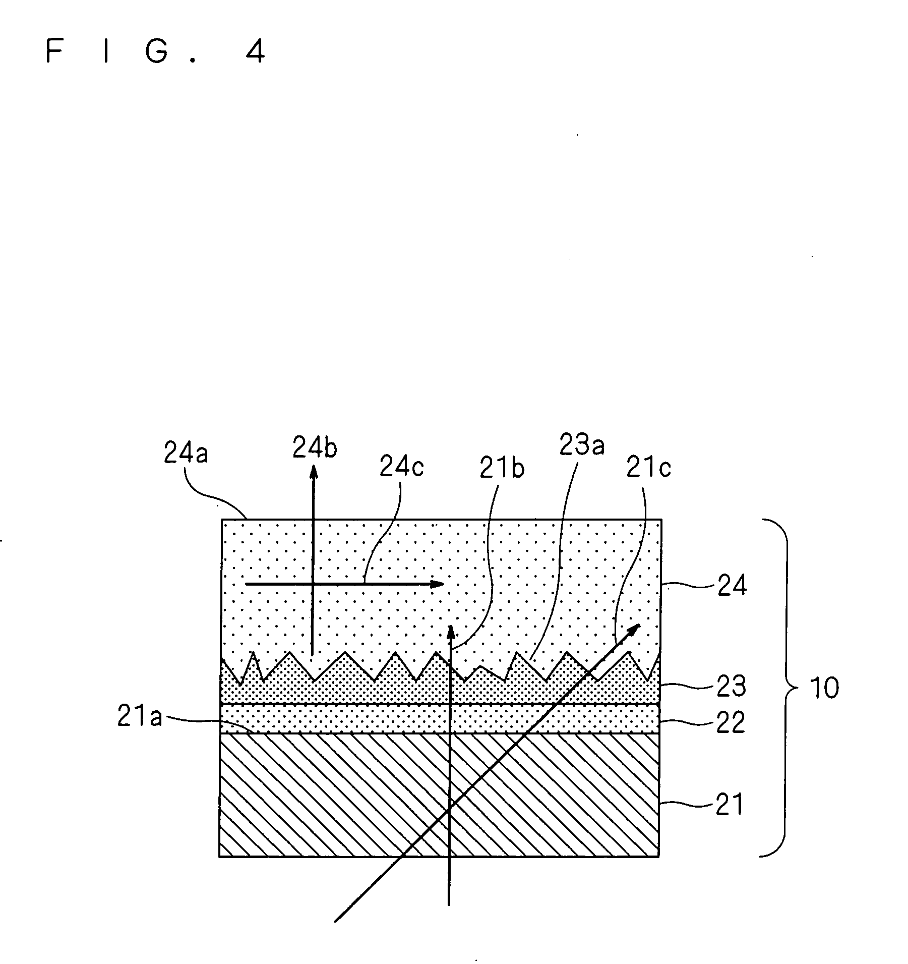
[0087]FIG. 4 is a sectional view showing an epitaxial substrate according to a second embodiment of the present invention. This epitaxial substrate is manufactured by forming a base layer22 and a first layer 23 successively on a principal plane 21a of the sapphire substrate 21 that has the principal plane on (01-12) plane (hereinafter referred to as R-plane sapphire substrate 21) by the MOVPE method. The first layer 23 receives a strain from the base layer 22, and therefore has the sectional plane thereof spontaneously generating irregular surface configuration 23a having period in a range from 10 nm to 20 μm and height in a range from 10 nm to 10 μm during crystal growth. Then a second layer 24 is grown so as to make the irregular surface configuration 23a formed on the first layer 23 smooth. As a result, root mean square surface roughness (hereinafter RMS) of the surface 24a of the second layer 24 becomes less than 10 nm. In case the irregular surface configuration 23a is not smoo...

third embodiment

[0106]FIG. 7 is a sectional view along the (11-20) plane that is the A plane of a sapphire substrate 35 of this embodiment. Accordingly, [0001] (denoted as c in the figure), that is the C axis, is inclined from the principal plane 36 of the sapphire substrate 35. The sapphire substrate 35 of the present invention has the principal plane 36, that is the R plane, inclined from (01-12) plane toward (0001) plane.

[0107] Definition of the off-angle α of inclining the (01-12) plane toward (0001) plane in the present invention is as follows. Off-angle α is the angle between the principal plane 36 of the sapphire substrate 35 and the (01-12) plane of sapphire. Since [0001] of sapphire which has hexagonal crystal system is uniquely determined, an Off-angle of the (01-12) plane approaching (0001) as denoted by “a” in the figure is defined as positive. On the other hand, an Off-angle of the (01-12) plane moving away from (0001) as denoted by “a′” in the figure is defined as negative.

[0108] Th...


PUM


Abstract

An epitaxial substrate for manufacturing field effect transistor (FET) that has heterojunction structure consisting of at least a channel layer made of gallium nitride or gallium indium nitride and a barrier layer made of aluminum gallium nitride formed successively on the principal plane of the sapphire substrate, wherein the principal plane of the sapphire substrate semiconductor is inclined from (01-12) plane toward (0001) plane by an off-angle α that is in a range of 0°<x≦5°. With this constitution, an epitaxial substrate for manufacturing field effect transistor having high smoothness is provided.

Description

BACKGROUND OF THE INVENTION [0001] 1. Field of the Invention [0002] The present invention relates to a sapphire substrate for growing a nitride semiconductor thereon, and an epitaxial substrate and a semiconductor device that utilize the same. [0003] 2. Description of Related Art [0004] Nitride semiconductors such as aluminum nitride (AlN), gallium nitride (GaN), indium nitride (InN) or aluminum indium gallium nitride (AlxGa1-x-yInyN(0≦x≦1, 0≦y≦1, 0≦x+y≦1)) that is a mixed crystal of the former ones, can be applied to light emitting or sensing device and electron device, and therefore have been widely studied in researches on the crystal growth and application to semiconductor devices. Some applications thereof to light emitting diode and laser diode have already been commercialized. [0005] Since nitride semiconductor cannot be grown into a large bulk of single crystal, it is usually hetero-epitaxially grown on a semiconductor growing substrate made of a different material such as (...

Claims


Application Information

Patent Timeline
IPC IPC(8): H01L29/22H01L33/16H01L33/32
CPCH01L29/045H01L29/2003H01L33/32H01L29/7787H01L33/16H01L29/66462
Inventor TSUDA, MICHINOBUIMURA, MASATAKAHONSHIO, AKIRAIWAYA, MOTOAKIKAMIYAMA, SATOSHIAMANO, HIROSHIAKASAKI, ISAMU
Owner KYOCERA CORP
Why Eureka
Try Eureka