Hologram element, production method thereof, and optical header

a technology of hologram elements and production methods, applied in the field of hologram elements, can solve the problems of inability to obtain desired alignment states, inability to impose desired electric fields on liquid crystal films, and difficulty in processing, so as to improve the productivity of hologram elements, prevent unnecessary scattering of light, and increase the accuracy of film thickness

Inactive Publication Date: 2006-03-16
RICOH KK
View PDF11 Cites 68 Cited by
  • Summary
  • Abstract
  • Description
  • Claims
  • Application Information

AI Technical Summary

Benefits of technology

[0087] In the present invention, because the isolation member also acts as a spacer, it is possible to increase the accuracy of the film thickness of the hologram element (that is, the gap between substrates). This can improve productivity of the hologram element.
[0088] In the present invention, because the isolation member is formed from a material capable of absorbing light of a wavelength of the light for exposure, it is possible to prevent unnecessary scattered light occurring during exposure with the interference light, unnecessary light due to multiple reflections between the substrates, which may degrade the hologram element. As a result, exposure of one isolated device region can be performed without being affected by unnecessary light, and the isolated region can be made small. This can improve productivity of the hologram element.
[0089] In the present invention, when fabricating the hologram element, specifically, when forming a film of the photo-sensitive recording material, the One Drop Fill (ODF) process is used, which allows a tiny quantity of the photo-sensitive recording material to be applied, for example, by inkjet. Therefore, the material can be applied to the isolated region in an appropriate amount, thereby forming a uniform film. This can reduce the number of processing steps compared to vacuum injection, and can improve productivity of the hologram element.
[0090] In the present invention, the isolation member may be formed from a conductive material, thus it is possible to apply an electric field between isolated regions. For example, when a dielectric-anisotropic liquid crystal is used as the photosensitive recording material, the liquid crystal alignment between the isolated regions can be controlled by the applied electric field; hence, it is possible to enlarge the birefringence of the liquid crystal in the hologram element. This large birefringence can improve the incidence angle dependence and wavelength dependence, and improve polarization dependence.
[0091] With the above hologram element of the present invention, it is possible to make an optical device compact, and improve overall performance of the device. For example, it is possible to make an optical header compact, reduce noise of an optical switch, and increase the brightness of a display.
[0092] In an optical header of the present invention, because the hologram element of the present invention is used as an optical element for deflecting the reflected light from the recording medium to the photo detector, by making the hologram element polarization dependent, the hologram element is able to transmit, reflect, diffract, or scatter the incident light according to the polarization direction of the incident light; therefore, on the light path of the light emitted from the light source, the light is more effectively condensed on the recording medium while diffraction essentially does not occur. On the returning light path (the polarization plane is rotated by 90°), light having information can be diffracted with a high diffraction efficiency. Therefore, it is possible to obtain a compact optical header having high light utilization efficiency.

Problems solved by technology

In the structures obtained by techniques disclosed in reference 7 and reference 8, in order to obtain high diffractive efficiency, grooves thereof have to be made deep, and this processing is difficult.
However, with reduced size of the electrode, if the thickness of the liquid crystal film is increased to increase the diffraction efficiency, the liquid crystal film may be even thicker than the pitch of the transparent electrode, and due to influence from neighboring electrodes, a desired electric field cannot be imposed on the liquid crystal film.
In addition, with a short pitch, the alignment state of the vertically aligned liquid crystal region may influence the adjacent horizontally aligned liquid crystal region, thus, desired alignment states cannot be obtained.
In the technique disclosed in reference 6, although it is possible to shorten the pitches of exposure, it is difficult to form short pitches as being exposed because of thermal diffusion of reactive active seeds.
However, this arrangement makes the structure of the device complicated, and causes a rise in the cost.
But, as described above, it is difficult to obtain a periodic structure as desired by etching processing.
However, because of the recording materials used in the above techniques of the related art, development processing of the photo resist is required; hence, a large number of fabrication steps are needed, and the productivity is low.
However, when using the polymerization reaction in liquid crystals (including the phase separation process), there exist problems in the spread of the reaction and in leakage of light due to multiple reflection.
Particularly, security-related techniques are attracting attention, and in these techniques, holograms which are more delicate and have higher resolution are required.
However, resolutions of mask exposure and laser beam direct writing are not high.
With the method of electron beam direct writing, although relatively high resolutions are obtainable, fabrication equipment is quite expensive, and thus the fabrication cost is high.
With the above methods, it is difficult to fabricate a single hologram having complicated characteristics by only one exposure, while by multiple exposures, it is possible to record (fabricate) plural holograms having different diffraction characteristics in a single hologram element.
In order to fabricate plural holograms the same as the above hologram, one has to repeat the positioning and fixing steps as many times as the number of the holograms to be fabricated; thus, a large number of fabrication steps and a large amount of fabrication time are needed.
Because multiple hologram photosensitive materials are used, the cost is high, and hence not suitable for mass production.
Further, similarly, in the course of forming the desired structure in exposure with the interference light, scattering, multiple reflections on the substrate interface along with a change of the refractive index of materials, noise light included in the master hologram, and other unnecessary light may influence the element being exposed or neighboring elements.

Method used


Image

  • Hologram element, production method thereof, and optical header
  • Hologram element, production method thereof, and optical header
  • Hologram element, production method thereof, and optical header

Examples


first embodiment

[0132] Below, descriptions are made of a configuration and operations of a hologram element of the present embodiment, and a method of producing the hologram element.

[0133] In the present embodiment, a polarization hologram element is used as an example, which has a periodic structure, the refractive index modulation of which changes with the polarization direction of incident light, and a method of producing such a polarization hologram element is described. More particularly, it is assumed that the polarization hologram element is fabricated by duplicating the hologram region of the periodic structure on a recording material by using a master hologram.

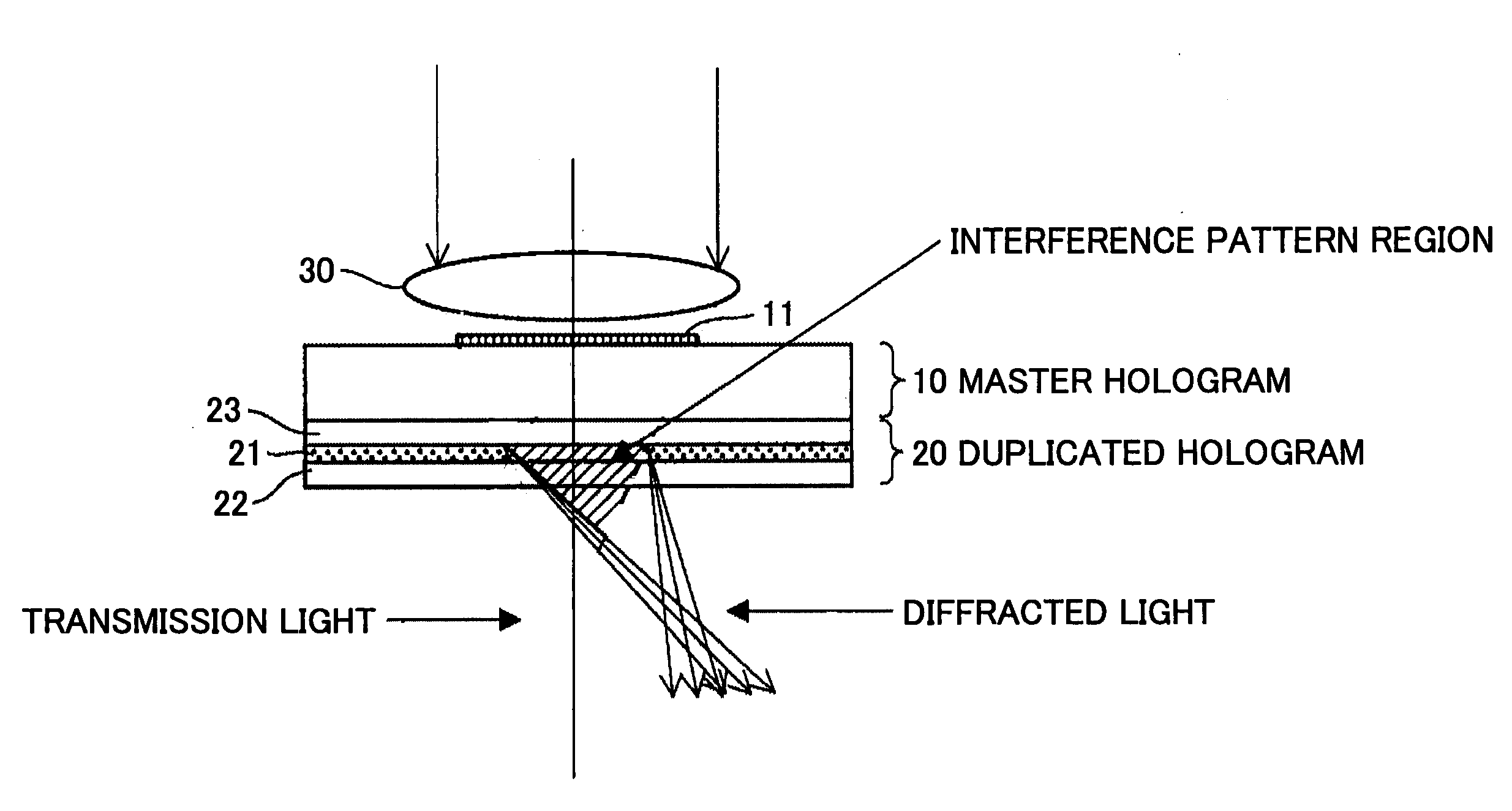
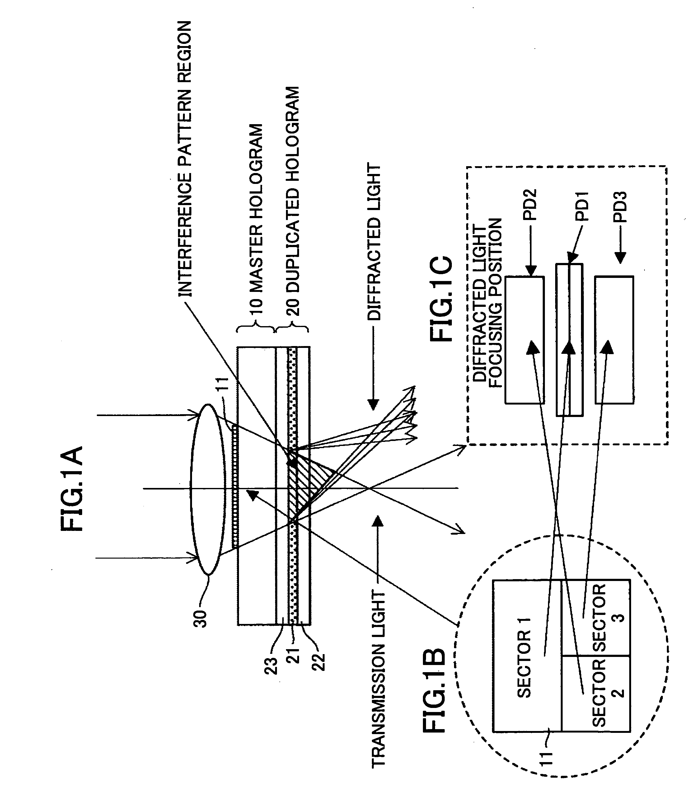
[0134]FIG. 1A through FIG. 1C are diagrams schematically illustrating a method of fabricating a polarization hologram element according to the present embodiment.

[0135] As illustrated in FIG. 1A, a master hologram 10 and a structure including substrates 22, 23 and a photo sensitive recording material 21 sandwiched by the substrate...

first example

FOR COMPARISON

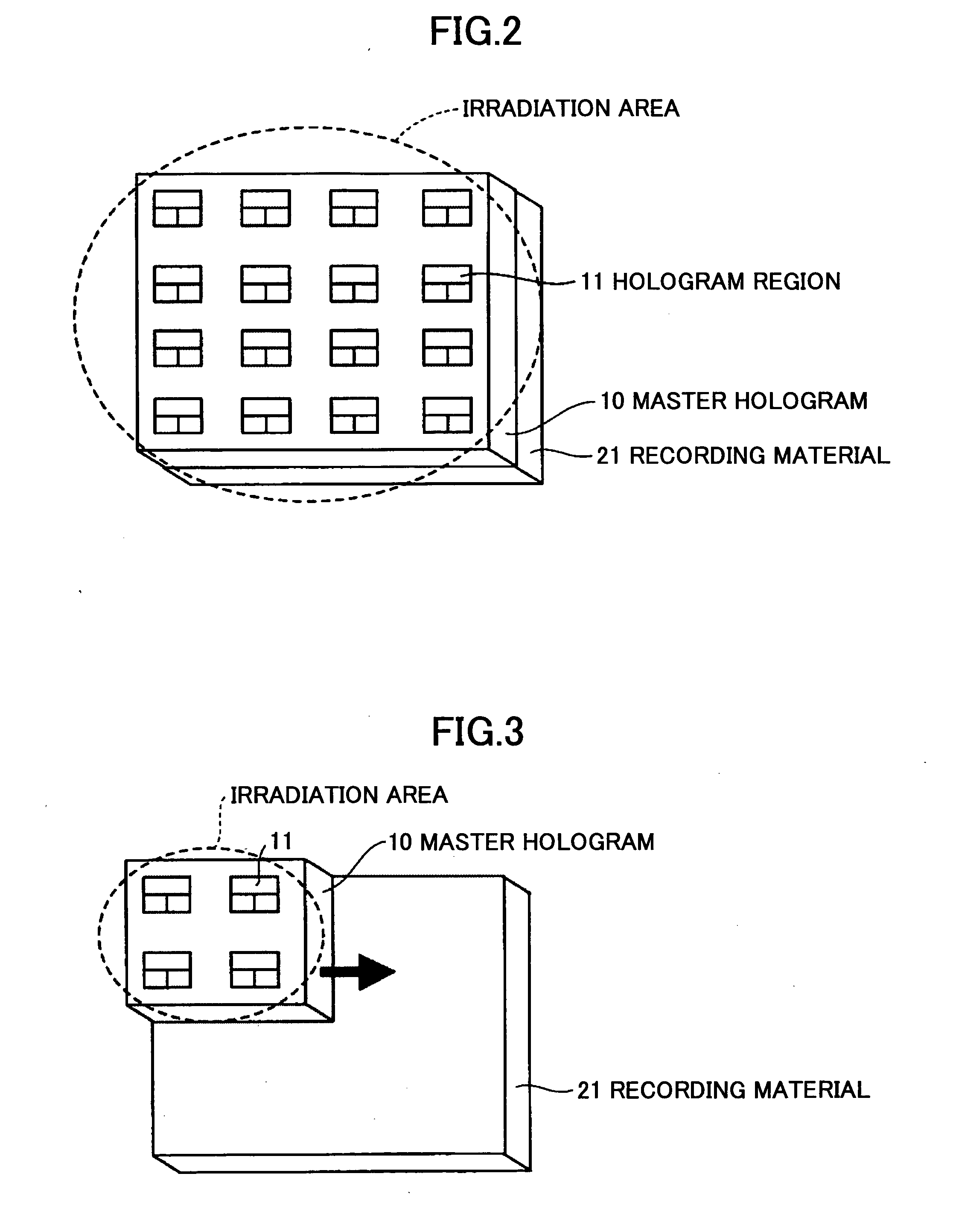
[0199]FIG. 13A and FIG. 13B are a plan view and a cross-sectional view of a master hologram produced by two-beam interference exposure using a photo resist.

[0200] When producing the master hologram 10 shown in FIG. 13A and FIG. 13B, the wavelength of the incident light is 442 nm, the ratio of the strength of the transmission light (zero-th order light) and the first order diffracted light is roughly 1:1, and in a region where two incident beams intersect each other, an interference pattern having a period of approximately 1 μm is formed. With this master hologram 10, a hologram is duplicated in a recording material as described below (photosensitive material) by exposure.

[0201]FIG. 14A and FIG. 14B are a plan view and a cross-sectional view exemplifying the hologram element 20 including a recording material sealed between two substrates.

[0202] As illustrated in FIG. 14A and FIG. 14B, in the hologram element 20, including the recording material 21 sealed between the ...

second example

FOR COMPARISON

[0227]FIG. 17A and FIG. 17B are a plan view and a cross-sectional view illustrating a cell (hologram element) 20 in which plural isolation members are provided.

[0228] As illustrated in FIG. 17A and FIG. 17B, two isolation members 24 are provided in the cell 20, and three isolated regions are formed. Except for this point, the cell 20 in the present example is the same as that in the example 2. The cell 20 holding the recording material is fabricated in the same way as in the example 2. In the present example, the opening area of the opening mask 40 is reduced corresponding to the isolated regions. Exposure and duplication are performed in each isolated region, that is, exposure and duplication are performed three times.

[0229] The obtained hologram element was evaluated in the same way as in the previous examples. In the test, diffracted light was observed in the hologram regions formed in the second and the third exposure, but not observed in the hologram region form...


PUM


Abstract

A method of producing a hologram element is disclosed that is able to prevent spread of a polymerization reaction and light leakage during exposure with interference light, and improve productivity in mass production. The hologram element is for transmitting, reflecting, diffracting, or scattering incident light, and includes a pair of substrates, an isolation member between the substrates that forms an isolated region, and a photo-sensitive recording material sealed in the isolated region. The hologram element includes a periodic structure formed by exposing the recording material to interference light. The interference light is generated by two or more light beams, or by using a master hologram. The recording material is formed from a composite material including a polymerized polymer or a polymerized liquid crystal. The periodic structure is formed by exposing the recording material to the interference light to induce the polymerization reaction and phase separation in the composite material.

Description

BACKGROUND OF THE INVENTION [0001] 1. Field of the Invention [0002] The present invention relates to a hologram element able to transmit, reflect, diffract, or scatter an incident light beam, and more particularly, to a hologram element which is dependent on the polarization state of the incident beam (thus referred to as a “polarization hologram element”), and is useful for reducing the size of an optical header for recording and reproducing data in an optical disk or a magneto-optical disk, or a hologram element which is able to improve light utilization efficiency of illumination light in an image display unit (for example, display units for reflection display by means of light transmission and scattering, or color display by means of light interference, or three-dimensional image display) or a projection display device, or a hologram element which is applicable to an optical switch for switching the light path of the incident beam depending on the polarization plane of the incid...

Claims


Application Information

Patent Timeline
Patent Type & Authority Applications(United States)
IPC IPC(8): G03H1/02
CPCG02B5/32G03H2260/33G03H1/0272G03H1/0486G03H1/202G03H2001/0264G03H2001/2276G03H2222/54G03H2227/04G03H2250/37G03H2260/12G03H2270/54G11B7/1353G11B7/22G03H1/02
Inventor KOBAYASHI, MASANORISUGIMOTO, HIROYUKIMIYAGAKI, KAZUYAFUNATO, HIROYOSHI
Owner RICOH KK
Why Eureka
Try Eureka