Method for making thin-film semiconductor device

a semiconductor device and thin film technology, applied in the direction of solid-state devices, laser beam welding apparatus, manufacturing tools, etc., can solve the problems of difficult to transfer glass substrates and increase equipment scale, process that can use plastic substrates is not easily achievable, and the desired productivity is not achieved. , to achieve the effect of preventing heat generation, reducing process steps, and reducing process temperatur

Inactive Publication Date: 2006-04-13
JAPAN DISPLAY WEST
View PDF7 Cites 13 Cited by
  • Summary
  • Abstract
  • Description
  • Claims
  • Application Information

AI Technical Summary

Benefits of technology

[0013] Thus, a method for making a thin-film semiconductor device including crystallizing an amorphous semiconductor thin film, the method using a further lower process temperature and streamlining the process steps, is desirable.
[0014] A method for making a thin-film semiconductor device includes an annealing step of irradiating an amorphous semiconductor thin film with a laser beam so as to crystallize the amorphous semiconductor thin film. In the annealing step, the semiconductor thin film is continuously irradiated with the laser beam while shifting the position of the semiconductor thin film irradiated with the laser beam at a predetermined velocity so that excess hydrogen can be removed from the region irradiated with the laser beam without evaporating and expanding hydrogen ions in the semiconductor thin film.
[0015] This method prevents heat generated in the semiconductor thin film due to the laser irradiation from affecting the substrate. By continuous irradiation with the laser beam, excess hydrogen in the region irradiated with the laser beam Lh diffuses from the solid side to the liquid side at the solid-liquid interface shifting a

Problems solved by technology

The drawback of this process is the difficulty of transferring the large glass substrate and the increased scale of equipment.
This temperature is higher than the heat resistant temperature of most plastic materials; hence, a process that can use the plastic substrate is not easily achievable even by the low-temperature polysilicon process.
Thus, in order to p

Method used


Image

  • Method for making thin-film semiconductor device
  • Method for making thin-film semiconductor device
  • Method for making thin-film semiconductor device

Examples


first embodiment

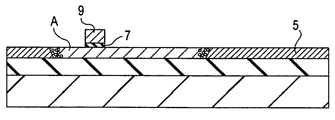
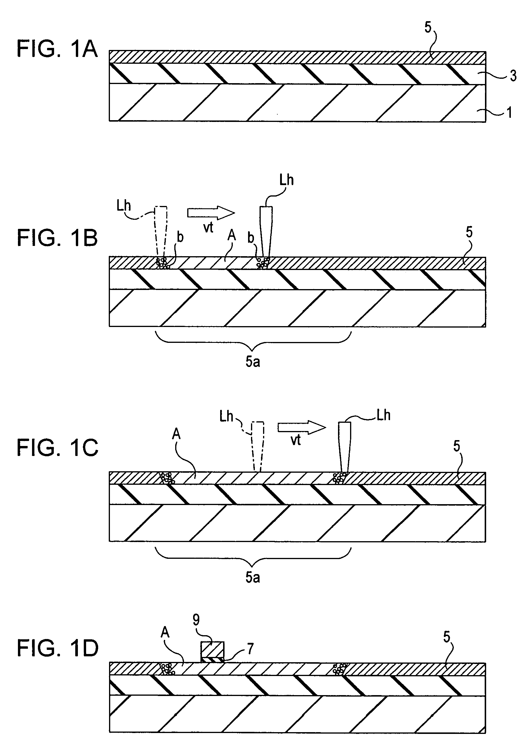
[0026]FIGS. 1A to 1D are cross-sectional views of process steps of a method for making a thin-film semiconductor device according to a first embodiment. The method of the first embodiment will be described with reference to FIGS. 1A to 1D.

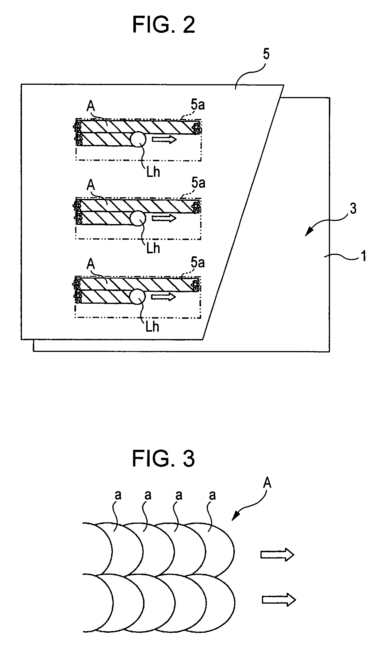
[0027] Referring first to FIG. 1A, a substrate 1 for forming a thin-film semiconductor device is prepared. The substrate 1 may be composed of glass, quartz, sapphire, plastic, or a metal, such as aluminum or stainless steel. An insulating buffer layer 3 for insulation is formed on a main face of the substrate 1 to prevent heat from conducting to the substrate 1. The detailed description of the substrate 1 and the buffer layer 3 are provided below.

[0028] An amorphous semiconductor thin film 5 made of amorphous silicon is then formed on the buffer layer 3 by a deposition process at a low deposition temperature. For example, plasma-enhanced chemical vapor deposition (PE-CVD) at a deposition temperature lower than 250° C., i.e., the heat resistant te...

second embodiment

[0074]FIGS. 6A to 6D are cross-sectional views of process steps of a method for making a thin-film semiconductor device according to a second embodiment. The method of the second embodiment will be described with reference to FIGS. 6A to 6D.

[0075] Referring first to FIG. 6A, a buffer layer 3 is formed on a substrate 1 in the same manner as the first embodiment described with reference to FIG. 1A. A semiconductor thin-film pattern 5a is formed on the buffer layer 3. The semiconductor thin-film pattern 5a has the same shape as the selected region 5a in the first embodiment. The semiconductor thin-film pattern 5a preferably has a shape including the selected region 5a described in the first embodiment and thus may be larger than the selected region 5a.

[0076] The semiconductor thin-film pattern 5a may be formed by a method in which the deposition temperature is low. As in the first embodiment, the semiconductor thin-film pattern 5a may be formed by pattern-etching a semiconductor thin...


PUM

PropertyMeasurementUnit
Diameteraaaaaaaaaa
Wavelengthaaaaaaaaaa

Abstract

A method for making a thin-film semiconductor device includes an annealing step of irradiating an amorphous semiconductor thin film with a laser beam so as to crystallize the amorphous semiconductor thin film. In the annealing step, the semiconductor thin film is continuously irradiated with the laser beam while shifting the position of the semiconductor thin film irradiated with the laser beam at a predetermined velocity so that excess hydrogen can be removed from the region irradiated with the laser beam without evaporating and expanding hydrogen ions in the semiconductor thin film.

Description

CROSS REFERENCES TO RELATED APPLICATIONS [0001] The present invention contains subject matter related to Japanese Patent Application JP 2004-286324 filed in the Japanese Patent Office on Sep. 30, 2004, the entire contents of which are incorporated herein by reference. BACKGROUND OF THE INVENTION [0002] 1. Field of the Invention [0003] The present invention relates to methods for making thin-film semiconductor devices and in particular to a method for making a thin-film semiconductor device, the method including an annealing step of crystallizing a semiconductor thin-film. [0004] 2. Description of the Related Art [0005] In flat-panel displays, such as liquid crystal displays (LCDs) and organic electro-luminescence (EL) displays, thin-film transistors (TFTs) are used as the switching element for a plurality of pixels of active matrix displays. The TFTs are categorized into polycrystalline silicon TFTs having active regions composed of polycrystalline silicon (poly-Si) or microcrystall...

Claims


Application Information

Patent Timeline
IPC IPC(8): H01L21/84
CPCH01L21/0242H01L21/02422H01L21/02488H01L21/02532H01L21/02576H01L21/0262H01L21/02675H01L21/02691H01L27/1214H01L27/1285B23K26/082B23K26/16H01L21/2026
Inventor MACHIDA, AKIOAKAO, HIROTAKAKAMEI, TAKAHIRONAKAO, ISAMU
Owner JAPAN DISPLAY WEST
Why Eureka
Try Eureka