Semiconductor device and method for manufacturing the same

a technology of semiconductor devices and semiconductor films, applied in semiconductor devices, semiconductor/solid-state device details, electrical equipment, etc., can solve the problems of difficult processing of copper (cu), difficult processing of wirings, and more significant irregularities in upper layers, so as to improve the adhesion between the interlayer insulating film and the paste containing ag, reduce the number of processes, and improve the effect of the quality

Inactive Publication Date: 2006-06-01
SEMICON ENERGY LAB CO LTD
View PDF34 Cites 43 Cited by
  • Summary
  • Abstract
  • Description
  • Claims
  • Application Information

AI Technical Summary

Benefits of technology

[0028] By selectively forming a wiring of the present invention, the number of the processes can be reduced compared with a conventional method. Further, a conductive film can be completely embedded in an interlayer insulating film having high aspect ratio by using a liquid conductive ma...

Problems solved by technology

In recent years, in the case of forming a multilevel interconnection which includes a plurality of wiring layer in a semiconductor element, irregularities are more significant in upper layers, and the wirings are difficult to be processed.
Further, it is difficult to process copper (Cu) by an etching process using an etchant or an etching gas; therefore, a special CMP method is required ...

Method used


Image

  • Semiconductor device and method for manufacturing the same
  • Semiconductor device and method for manufacturing the same
  • Semiconductor device and method for manufacturing the same

Examples


embodiment mode 1

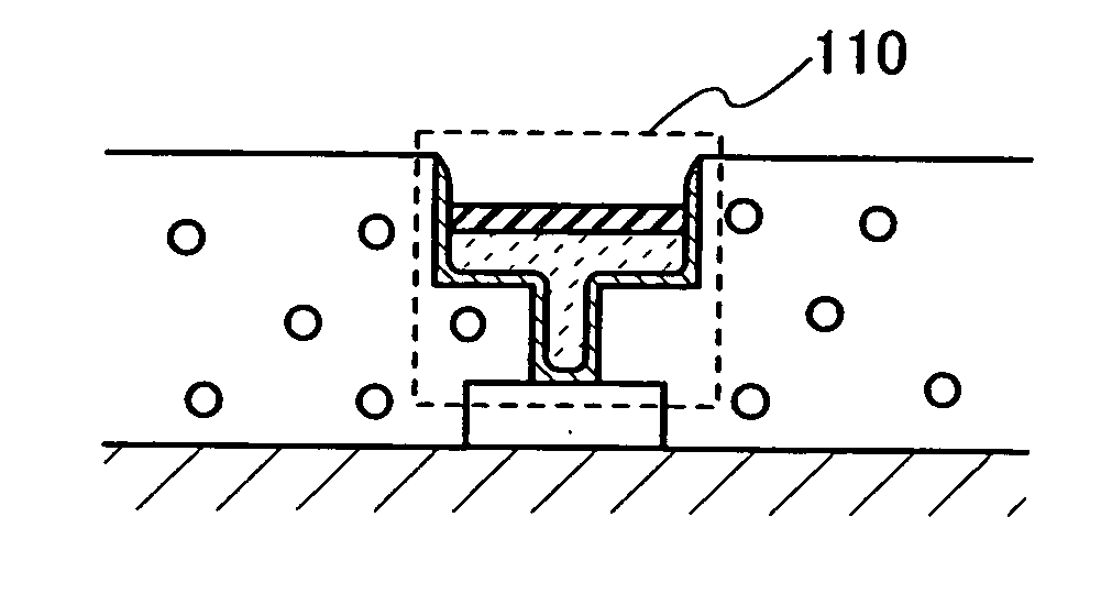
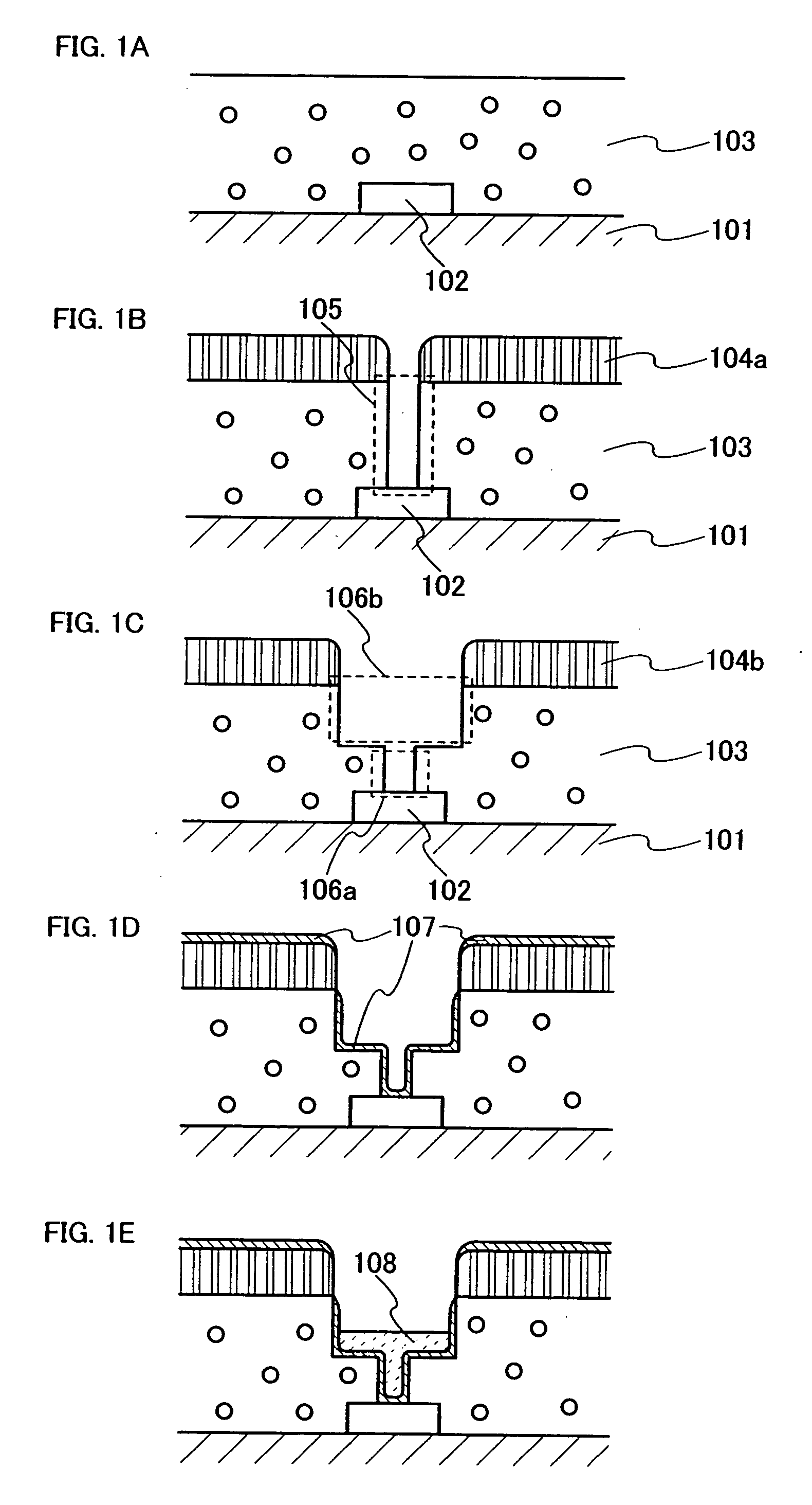
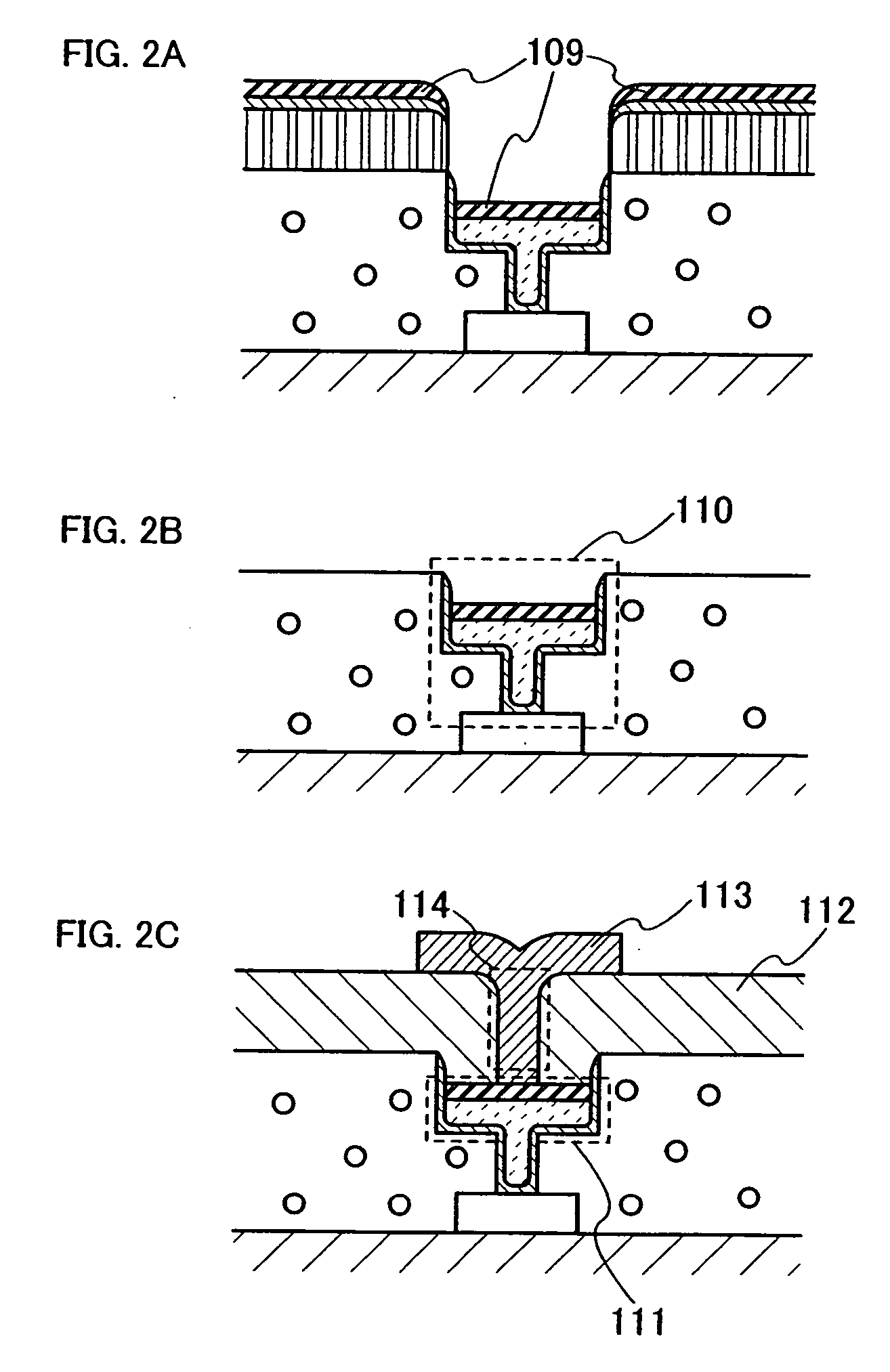
[0039] In this embodiment mode, modes of forming a silver wiring embedded in an interlayer insulating film in accordance with the present invention will be described with reference to FIGS. 1A to 1E and FIGS. 2A to 2C. Here, semiconductor elements and integrated circuits are not shown for simplicity, and only a connection portion of an embedded silver wiring and a lower layer wiring is shown.

[0040] First, a first layer wiring (a lower layer wiring) 102 is formed over an insulating film 101 provided over a semiconductor substrate in which elements such as a transistor (not shown) are formed. An interlayer insulating film 103 is formed to cover the wiring 102 (FIG. 1A).

[0041] The semiconductor substrate is a single crystal silicon substrate or a chemical compound semiconductor substrate. An n-type or p-type single crystal silicon substrate, a GaAs substrate, an InP substrate, a GaN substrate, a SiC substrate, a sapphire substrate, or a ZnSe substrate is typically used. Further, an S...

embodiment mode 2

[0059] In this embodiment mode, one mode of the present invention in which part of the process is different from the above Embodiment Mode 1 will be described with reference to FIGS. 3A to 3F. Here, semiconductor elements and integrated circuits are not shown for simplicity, and only a connection portion of an embedded silver wiring and a lower layer wiring is shown as in FIGS. 1A to 1F.

[0060] First, steps of from FIG. 1A to FIG. 1C are conducted as in Embodiment Mode 1. Subsequently, the mask is removed to obtain the state shown in FIG. 3A. FIG. 3A shows a lower layer wiring 202 and an interlayer insulating film 203 which are formed over an insulating film 201 provided over a semiconductor substrate in which elements such as a transistor (not shown) are formed, and a connection hole 204a and a wiring trench 204b which are provided in the interlayer insulating film 203.

[0061] Next, a barrier film 205 is formed over the entire surface by sputtering or CVD as shown in FIG. 3B. The i...

embodiment 1

[0071] A procedure for manufacturing an FET using the present invention will be hereinafter described simply with reference to FIG. 4. Here, an example of using a wiring connected to an impurity region of the FET as a lower layer wiring to form an embedded wiring in a porous insulating film covering the lower layer wiring is shown.

[0072] A silicon substrate 301 formed of single crystal silicon is prepared. An n-well 302 is formed in a first element formation region in a main surface (also referred to as an element formation surface or a circuit formation surface) of the silicon substrate, and a p-well 303 is formed in a second element formation region in the same surface.

[0073] Next, a field oxide film 306 to be an element isolation region for partitioning the first element formation region and the second element formation region is formed. The field oxide film 306 is a thick thermal oxide film and may be formed by known LOCOS. Note that the element isolation method is not limited...


PUM


Abstract

In a manufacturing process of a semiconductor device, electroplating and CMP have had a problem of increase in manufacturing costs for forming a wiring. Correspondingly, an opening is formed in a porous insulating film after a mask is formed thereover, and a conductive material containing Ag is dropped into the opening. Further, a first conductive layer is formed by baking the conductive material dropped into the opening by selective irradiation with laser light. Subsequently, a metal film is formed over the entire surface by sputtering, and the mask is removed thereafter to have only the metal film remain over the first conductive layer, thereby forming an embedded wiring layer formed with a stack of the first conductive layer containing Ag and the second conductive layer (metal film).

Description

BACKGROUND OF THE INVENTION [0001] 1. Field of the Invention [0002] The present invention relates to a semiconductor device having an integrated circuit and a method for manufacturing the same. The invention particularly relates to an electronic device having, as a component, a semiconductor element including an embedded wiring. [0003] Note that a semiconductor device in this specification means general devices and apparatuses which can function with the use of semiconductor characteristics; for example, electro-optical devices, semiconductor circuits, and electronic devices are all included in a semiconductor device. [0004] 2. Description of the Related Art [0005] In recent years, in the case of forming a multilevel interconnection which includes a plurality of wiring layer in a semiconductor element, irregularities are more significant in upper layers, and the wirings are difficult to be processed. Correspondingly, a wiring material is generally embedded in a wiring opening such a...

Claims


Application Information

Patent Timeline
IPC IPC(8): H01L23/52H01L21/4763
CPCH01L21/288H01L21/76843H01L21/76849H01L21/76852H01L21/76862H01L21/76864H01L21/76874H01L21/76877H01L21/7688H01L23/5222H01L23/53242H01L23/53252H01L23/5329H01L2224/45144H01L2224/32225H01L2224/48091H01L2224/48227H01L2224/73265H01L2924/15184H01L2924/15311H01L2924/00014H01L24/45H01L2924/00012H01L2224/45015H01L2924/12044H01L24/73H01L2924/181H01L2924/14H01L2924/00
Inventor ISA, TOSHIYUKIYAMAZAKI, SHUNPEI
Owner SEMICON ENERGY LAB CO LTD
Why Eureka
Try Eureka