Nanocontact printing

a technology of nano-contact printing and printing plate, which is applied in the field of nano-contact printing, can solve the problems of inability to scale up production, inability to meet the needs of customers, etc., and achieve the effect of constant production of masters

Inactive Publication Date: 2006-06-29
MASSACHUSETTS INST OF TECH
View PDF21 Cites 58 Cited by
  • Summary
  • Abstract
  • Description
  • Claims
  • Application Information

AI Technical Summary

Benefits of technology

[0018] A unique feature of the method of the invention is the ability to copy, and thus replicate, the master itself using the parallel method of the invention instead of the methods of the prior art in which printed items cannot act as a master. This is a major advantage over any existing methods. In fact, typically for large production lines many masters are needed. This, combined with the wearing of existing molds, means that a constant production of masters is required. In the method of the invention, once a master is produced, reproductions of the master can be produced from it, and these new master will then be used to print the final devices. Reproducibility should be improved and, more importantly the instruments for the primary master fabrication which produce features in a serial fashion will have to be used only to fabricate the primary master.

Problems solved by technology

Furthermore, the typical disadvantages of organic materials are less important in nanodevices; for example, there is less need for good mechanical properties or high thermal stability.
Unfortunately, all nano-lithographies have in common the same drawback: they are extremely slow, and it has been postulated that device fabrication time (and reproducibility) will be the main limiting factor in nanotechnology.
In particular, the problem of how to scale up production has not been solved.
Unfortunately, micro-contact printing has serious resolution limitations, so its application in nanotechnology is limited.
In fact, the main limitations to nano-imprint is that it needs a “hard” mold and that it is tailor-made to print a shape on a silicon wafer.
It is difficult to envision how such a method could be adapted for soft molds (i.e., a mold made of an organic material) and / or how it could be used to transfer the high degree of complexity and information that an organic (particularly a bio-organic) substrate can carry.
A major drawback of existing nanolithography techniques for fabricating nanoscale devices is that features of the device must be fabricated in a series of steps.
Thus, these techniques are limited to relatively simple devices since the fabrication of devices having many features would take a prohibitive amount of time.

Method used


Image

  • Nanocontact printing
  • Nanocontact printing
  • Nanocontact printing

Examples


example 1

Preparation of a Complement Image of a DNA Monolayer

[0100] A. Preparation of DNA Solutions

[0101] All glassware was cleaned with a solution of 75% H2SO4 and 25% H2O2 before use. All water used was ultrapure water (18MΩ / cm).

[0102] The primary DNA, 5′- / 5-ThiolMC6-D / ACG CAA CTT CGG GCT CTT-3′, were purchased from Integrated DNA Technologies, Inc. (IDT), Coraville, Iowa. All DNA strands were used as received from the manufaturer. The primary DNA was dissolved in water at the concentration of 1 μg / mL and divided into smaller aliquots of 50 μL, and stored at −20° C. When a portion of this solution was used, an aliquot was reduced by placing it in a 40 mM buffer solution (0.17 M sodium phosphate, pH 8) having dithiothreitol (DTT) for 16 hr. The oligonucleotides were separated from the by-products of the DTT reaction using size exclusion chromatography (NAP 10 column from Pharmacia Biotech) following the manufactures instructions. 10 mM sodium phosphate buffer (pH 6.8) was used to equilib...

example 2

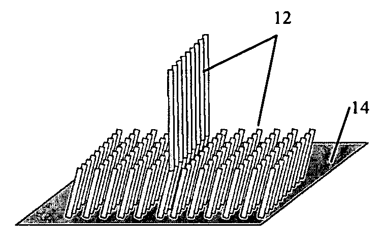
Pattern Transfer of Gold Grid

[0111] An AFM calibration gold grid was dipped in 4 μM solution of the primary DNA molecules described in Example 1 for 5 days to generate a patterned master. The master was exposed to 1 mM 6-mercapto-1-hexanol aqueous solution for 2 hr to minimize nonspecific adsorption of single-stranded DNA, then rinsed with water 5 times and air-dried. The master was then exposed to a 6 μM solution of the secondary DNA described in Example 1 for 2 hours so that hybridization occurred. A second substrate of gold on mica was placed on the master so that the two gold surfaces were facing each other and had a small amount of water in between them. A small mechanical force was applied to force the two substrates together. After about 5 hr, the substrates were dipped into 1M NaCl in TE buffer solution (70° C.) for 20 min. The two substrates (i.e., master and the complement image) spontaneously separated and were rinsed with 1M NaCl in TE buffer 2 times and with water 5 ti...

example 3

Fabrication of a DNA Chip

[0112] A master is prepared using Dip Pen Nanolithography, as described in Demer, et al., Angew. Chem. Int. Ed. (2001), 40:30713073, the entire teachings of which are incorporated herein by reference. To prepare the master, a surface of a gold on mica substrate is contacted with a 1 mM solution of 1-octadecanethiol (ODT) in ethanol for 5 min. to cover the exposed gold surface with ODT molecules. The substrate is then immersed in a 1 mM solution of 1,16-mercaptohexadecanoic acid (MHA) and the tip of an atomic force microscope is used to displace ODT molecules bound to the surface by contacting the surface with a force of about 0.5 nN making a 100 nm dot. The MHA in solution binds to the exposed gold surface of the dot. The carboxylic acid groups of the MHA are activated with a 10 mg / mL solution of 1-ethyl-3-(3-dimethylaminoproppyl)carbodiimide hydrochloride (EDAC) in 0.1M morpholine / ethanesulfonic acid at pH 4.5, and then rinsed with a solution of 0.1M sodiu...


PUM

PropertyMeasurementUnit
areaaaaaaaaaaa
dissociation constantaaaaaaaaaa
concentrationaaaaaaaaaa

Abstract

A method of stamping of molecular patterns and/or devices based on the reversible self-assembly of molecules, particularly organic molecules is disclosed. This method is suitable for the stamping of almost any nanofabricated device and can be used to transferring a large amount of pattern information from one substrate to another at the same time.

Description

BACKGROUND [0001] In recent years, there has been considerable effort aimed at understanding new phenomena in the nanoscale, a diversity of new nanostructured materials have been fabricated and characterized. New devices with intriguing properties are just beginning to be engineered. The expectations for a new generation of cheap and innovative tools that will change our lives are very high. The combination of a new set of expected and unexpected properties together with a whole new family of materials and fabrication methods will enable devices that we could not even have conceived just ten years ago. Coulomb blockade in metal nanoparticles as well as in semiconductor quantum dots, narrow band fluorescence emission from semiconductor nanoparticles, quantized ballistic conduction in nanowires and nanotubes: these are just a few new materials / phenomena that will have an impact on the way we design optical and electronics devices. For a review of nanodevices and fabrication techniques...

Claims


Application Information

Patent Timeline
Patent Type & Authority Applications(United States)
IPC IPC(8): B32B5/02
CPCB82Y10/00B82Y30/00Y10T428/268G03F7/0002B82Y40/00Y10T428/31536
Inventor STELLACCI, FRANCESCOYU, ARUM
Owner MASSACHUSETTS INST OF TECH
Why Eureka
Try Eureka