Manufacturing method of laser processed parts and adhesive sheet for laser processing

a manufacturing method and laser processing technology, applied in metal-working equipment, electrical equipment, lamination, etc., can solve the problems of inability to meet the demand, difficulty in postprocessing removal of decomposition products, and inability to drill or die conventionally, etc., to achieve easy recovery of workpieces after processing, effective suppression of contamination of workpiece surfaces, and high speed

Inactive Publication Date: 2006-07-20
NITTO DENKO CORP
View PDF40 Cites 33 Cited by
  • Summary
  • Abstract
  • Description
  • Claims
  • Application Information

AI Technical Summary

Benefits of technology

[0008] An object of the present invention to provide a method of manufacturing a laser processed part capable of processing at high precision and high speed when processing a workpiece by optical absorption ablation of a laser beam, effectively suppressing contamination of a workpiece surface by decomposition products, and easily recovering the workpiece after processing. It is another object to provide an adhesive sheet for laser processing used in the method of manufacturing the laser processed part.

Problems solved by technology

In the conventional press processing or blanking process, the precision is about ±100 μm at most, and such demand cannot be satisfied.
Drilling of materials is also demanded to conform to high definition and high precision, and drilling by using conventional drill or die cannot meet the needs.
Adhesion strength of the decomposition products becomes stronger in proportion to the power of the laser beam, and when the laser beam power is increased, it tends to be difficult to remove the decomposition products in postprocessing.
Accordingly, a problem has been noted that an improvement of processing throughput by increasing the laser power may be hindered, or processing precision may be lowered.
Moreover, if the dicing sheet is also cut off when cutting the workpiece, the laser processed part drops off.
Therefore, there is also a problem that a certain portion must be kept uncut when cutting, which makes the handling performance poor.
When using the dicing sheet disclosed in Japanese Patent Application Laid-Open No. 2002-343747, the adhesive layer is thermally cut off by the fundamental wave of YAG laser (wavelength 1064 nm) or a laser beam of ruby laser (wavelength 694 nm), and decomposition products of an adhesive layer may invade into the interface between the dicing sheet and the workpiece, and may stick stubbornly to the interface area.
As a result, there is a problem that it is hard to remove the dicing sheet from the workpiece after laser processing, or laser-processing precision is lowered.
However, when the adhesive tape is applied in a method of dicing a semiconductor wafer by using only a laser, due to the heat by the laser irradiation, the adhesive layer or base material may be dissolved, and decomposition products of the adhesive layer and the base material may invade into the interface between the adhesive sheet and the semiconductor wafer, sticking stubbornly to the interface area, and similar problems may occur.
Further, when water microjet is used, there is a limit in reducing the cutting width since the cutting width in dicing is defined by the diameter of the water jet, and thus it is inferior in the aspect of manufacturing efficiency of semiconductor chip.

Method used


Image

  • Manufacturing method of laser processed parts and adhesive sheet for laser processing
  • Manufacturing method of laser processed parts and adhesive sheet for laser processing
  • Manufacturing method of laser processed parts and adhesive sheet for laser processing

Examples


example 1

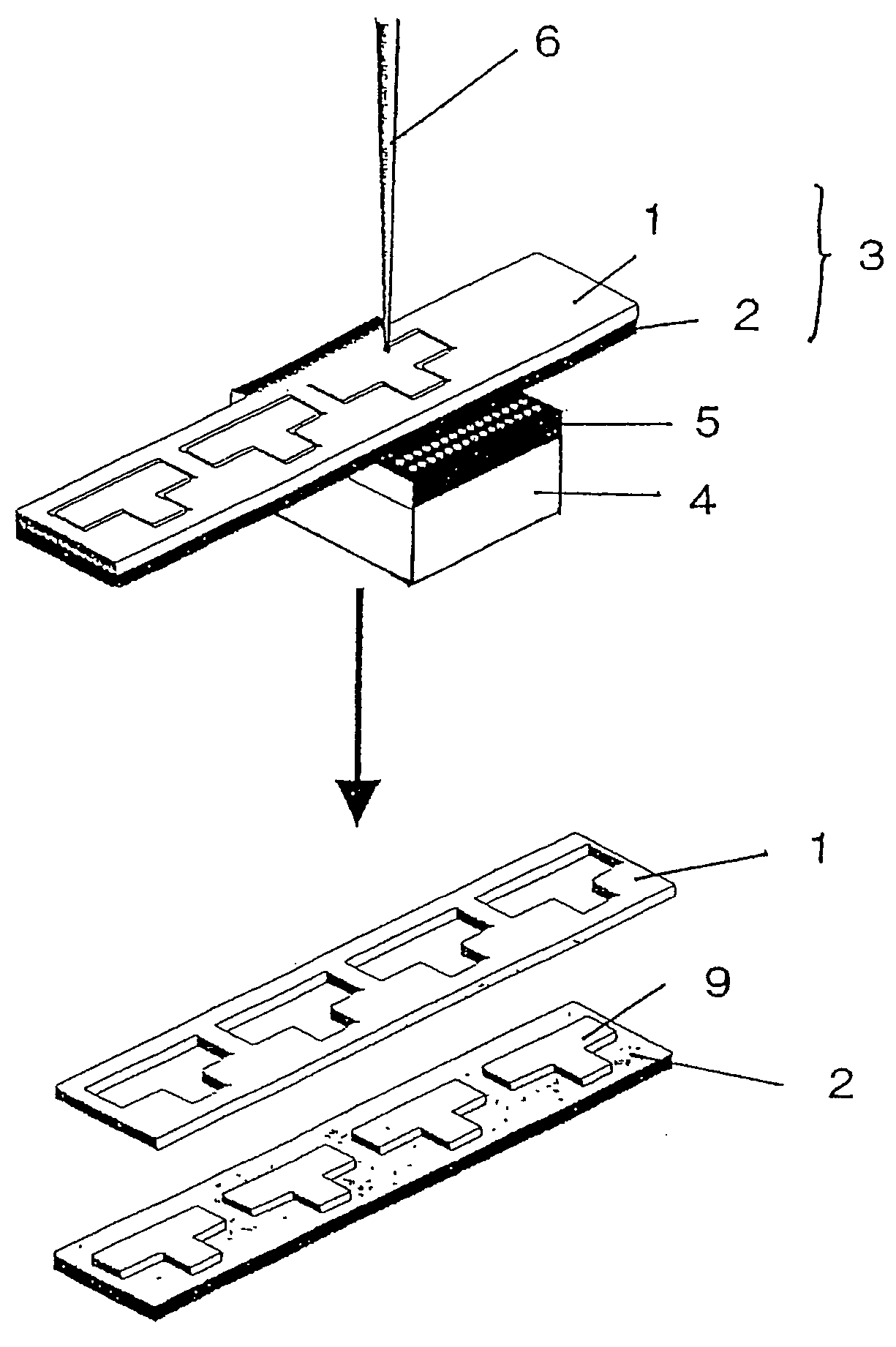
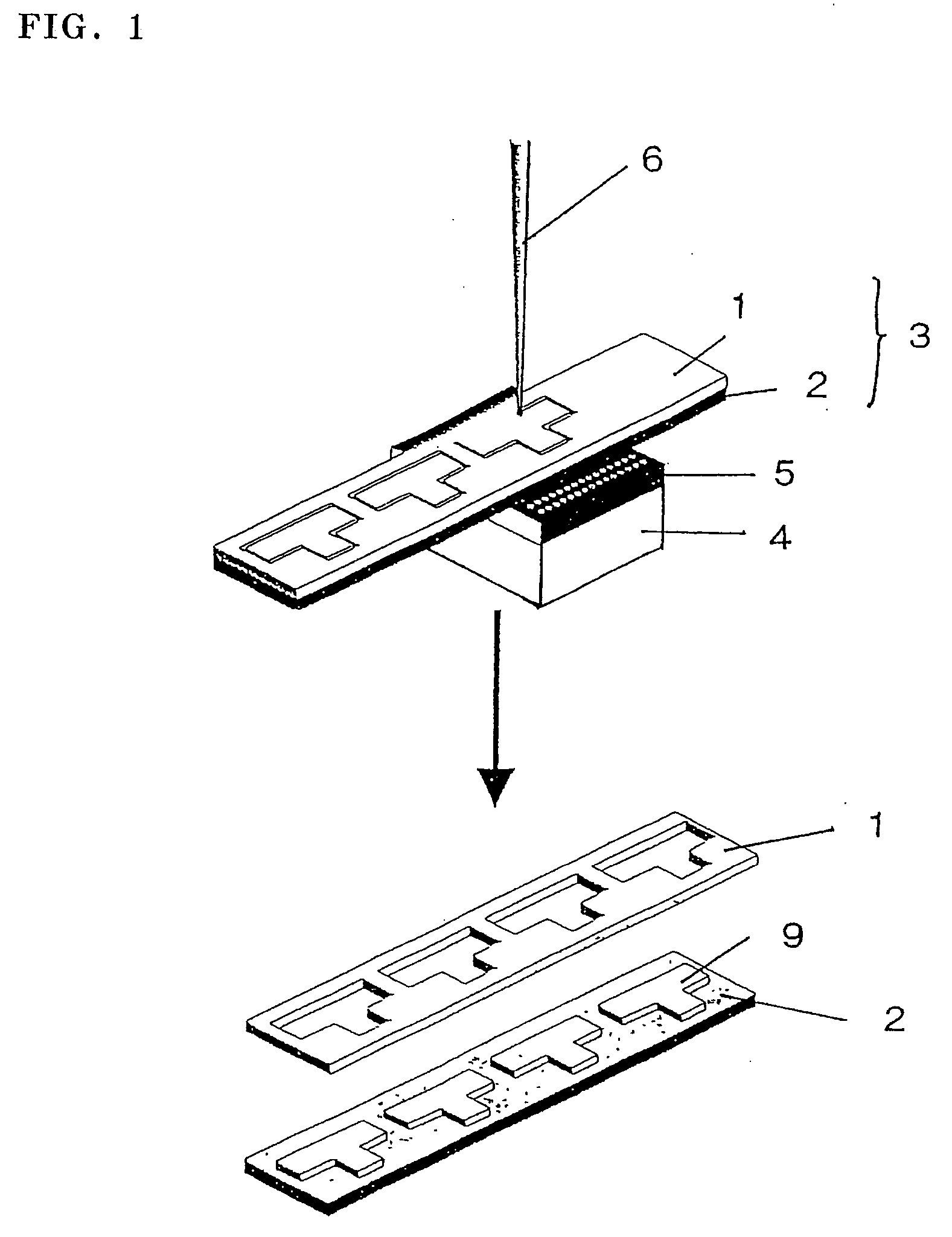
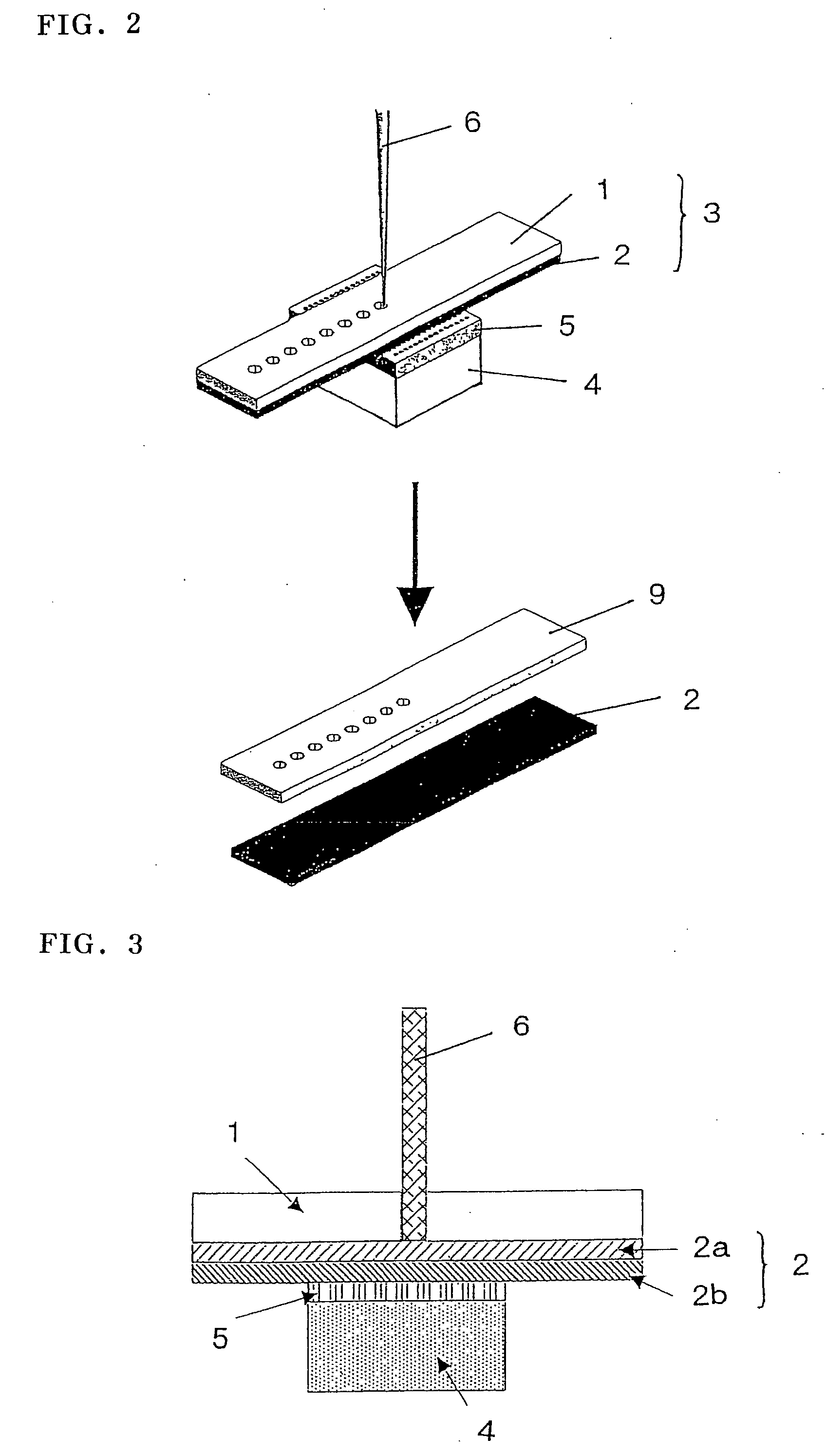
[0082] Acrylic adhesive solution (1) was applied and dried on a base material (thickness 50 μm) made of ethylene-vinyl acetate copolymer, and an adhesive layer (thickness 10 μm) was formed, and an adhesive sheet for laser processing was obtained. Extinction coefficient of adhesive sheet was 8.6 cm−1.

[0083] Acrylic adhesive solution (1) was prepared in the following method. Acrylic adhesive solution (1) was prepared by adding 100 parts by weight of acrylic polymer of number-average molecular weight of 800,000 prepared by copolymerization of butyl acrylate / ethyl acrylate / 2-hydroxy ethyl acrylate / acrylic acid at ratio by weight of 60 / 40 / 4 / 1, 90 parts by weight of dipentaerythritol monohydroxy pentacrylate as photopolymerizable compound, 5 parts by weight of benzyl dimethyl ketal (Irgacure 651) as photopolymerization initiator, and 2 parts by weight of polyisocyanate type cross-linking agent (Coronate L manufactured by Nippon Polyurethane Co.) to toluene, and dissolving and mixing un...

example 2

[0089] Adhesive sheet for laser processing was manufactured in the same procedure as in example 1, except that base material of polymethyl methacrylate (thickness 100 μm) was used instead of ethylene-vinyl acetate copolymer. The extinction coefficient of adhesive sheet was 1.7 cm−1.

[0090] Using the adhesive sheet for laser processing, it was cut and processed in the same manner as in example 1, except that silicon wafer (thickness 75 μm) was used instead of polyurethane sheet as material to be processed. At this time, silicon wafer was cut off, but the base material of adhesive sheet was not processed at all. Ultraviolet ray was emitted to adhesive sheet, and adhesive layer was cured. The adhesive sheet was peeled off, and the laser processing peripheral area of adhesive sheet adhering surface (laser beam exit side) of silicon wafer was observed, but decomposition product (deposit) of base material and adsorption board was not observed.

[0091] As clear from the examples and compara...


PUM

PropertyMeasurementUnit
extinction coefficientaaaaaaaaaa
wavelengthaaaaaaaaaa

Abstract

Providing a method of manufacturing a laser processed part capable of processing at high speed and high precision when processing a workpiece by optical absorption ablation of laser beam, effectively suppressing contamination of a workpiece surface by decomposition products, and recovering the workpiece easily after processing. Another object is to present an adhesive sheet for laser processing preferably used in the method of manufacturing a laser processed part.

Description

TECHNICAL FIELD [0001] The invention relates to a manufacturing method of laser processed parts obtained by processing workpieces such as sheet material, circuit board, semiconductor wafer, glass substrate, ceramic substrate, metal substrate, semiconductor laser or other light emitting and light detecting element board, MEMS board, semiconductor package, cloth, leather, paper or the like, by cutting, drilling, marking, grooving, scribing, trimming or other shaping process by ultraviolet absorption ablation by laser beam. The present invention also relates to an adhesive sheet for laser processing used when processing a workpiece by ultraviolet absorption ablation by laser beam. BACKGROUND ART [0002] As the electronic and electric appliances are reduced in size recently, component parts are also reduced in size and advanced in definition, and high definition and high precision are demanded in machining of parts at machining precision of ±50 μm or less. In the conventional press proce...

Claims


Application Information

Patent Timeline
Patent Type & Authority Applications(United States)
IPC IPC(8): B32B38/00B32B38/04B26D1/00H01L21/301H01L21/78
CPCB23K26/38Y10T156/108B23K26/4005B23K26/403B23K26/4075B23K26/408B23K2201/40H05K3/0026B23K26/385B23K26/401B23K26/4015B23K26/402B23K2203/04B23K2203/10B23K2203/12B23K26/404B23K26/4055B23K26/406B23K26/4065B23K26/4085B23K26/409B23K2203/02B23K2203/14Y10T156/1057Y10T156/1082Y10T156/1052B23K26/381B23K26/40B23K26/382B23K26/389B23K2103/54B23K2101/40B23K2101/42B23K2103/02B23K2103/05B23K2103/08B23K2103/10B23K2103/12B23K2103/14B23K2103/16B23K2103/172B23K2103/26B23K2103/34B23K2103/38B23K2103/40B23K2103/42B23K2103/50B23K2103/52B23K2103/56Y10T83/04Y10T83/0405
Inventor MATSUO, NAOYUKIURAIRI, MASAKATSUHINO, ATSUSHI
Owner NITTO DENKO CORP
Why Eureka
Try Eureka