

Memory element using active layer of blended materials
- Summary
- Abstract
- Description
- Claims
- Application Information
AI Technical Summary
Benefits of technology
Problems solved by technology
Method used
Image

Examples
Embodiment Construction
[0023] Reference is now made in detail to a specific embodiment of the present invention which illustrates the best mode presently contemplated by the inventors for practicing the invention.
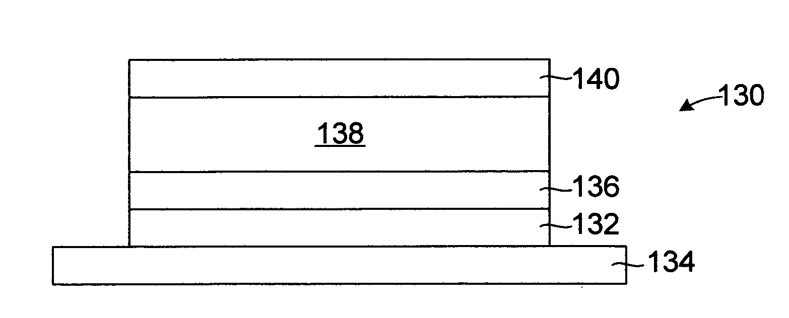
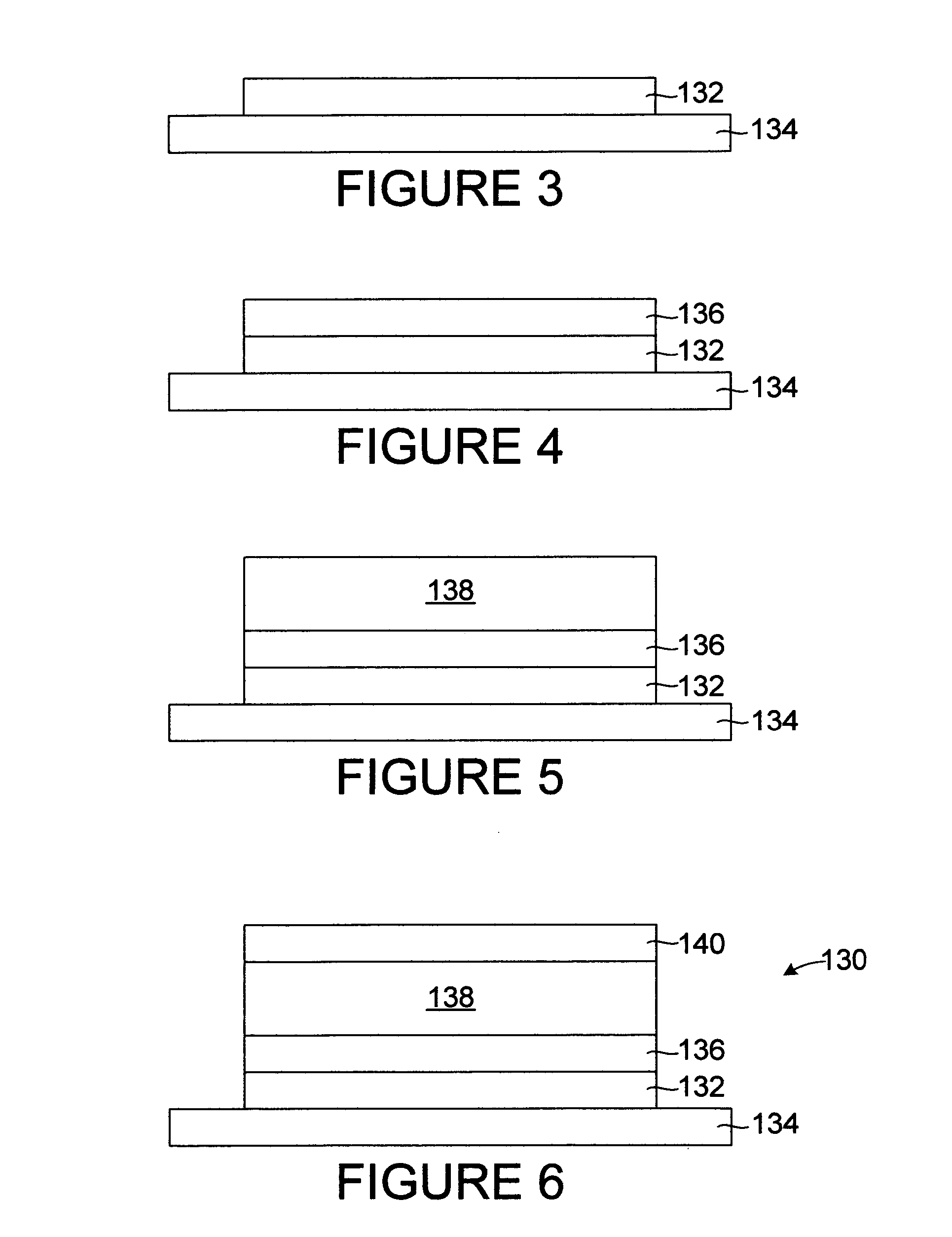
[0024]FIGS. 3-6 illustrate a process for fabricating a first embodiment of memory element 130 in accordance with the present invention. Initially, an electrode 132 is formed on a substrate 134 (FIG. 3). The electrode 132 may be formed by any suitable technique, such as physical vapor deposition, i.e. PVD (such as thermal vacuum evaporation, e-beam deposition or sputtering), ion plating, chemical vapor deposition, i.e. CVD (such as metal-organic CVD, i.e. MOCVD), plasma-enhanced CVD, i.e. PECVD, and the like. The electrode 132 in this embodiment is copper, but it will be understood that the electrode 132 can be formed of any of a number of materials including aluminum, barium, calcium, chromium, cobalt, copper, germanium, gold, magnesium, manganese, molybdenum, indium, iron, nickel, palladium, pl...
PUM
 Abstract
Description
Claims
Application Information