

Field effect transistor and method of manufacturing the same
- Summary
- Abstract
- Description
- Claims
- Application Information
AI Technical Summary
Benefits of technology
Problems solved by technology
Method used
Image

Examples
synthesis example 1
Synthesis of Bicyclo Compound
Step (1)
[0048] A mixed solution of 3.16 g (39.5 mmol) of 1,3-cyclohexadiene, 10.5 g (34.05 mmol) of trans-1,2-bis(phenylsulfonyl)ethylene, and 200 ml of toluene was refluxed for 7 hours. Then, the mixed solution was cooled and concentrated under reduced pressure to yield a reaction mixture. The reaction crude product was recrystallized (chloroform / hexane) to yield 5,6-bis(phenylsulfonyl)-bicyclo[2,2,2]octa-2-ene (13.8 g, 35.6 mmol, 90% yield).
Step (2)
[0049] A reaction system of a mixed solution of 7.76 g (20 mmol) of the resultant 5,6-bis(phenylsulfonyl)-bicyclo[2,2,2]octa-2-ene and 50 ml of anhydrous tetrahydrofuran was replaced with nitrogen. Then, 2.425 ml (22 mmol) of ethyl isocyanoacetate were added to the mixed solution, and the whole was cooled to 0° C. Potassium tert-butoxide (50 ml / l M THF solution) was dropped into the mixture in 2 hours, and the whole was stirred at room temperature for 3 hours. After the completion of the reaction, dil...
example 1
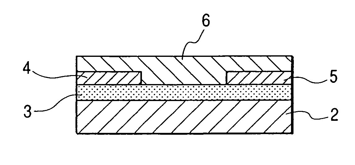
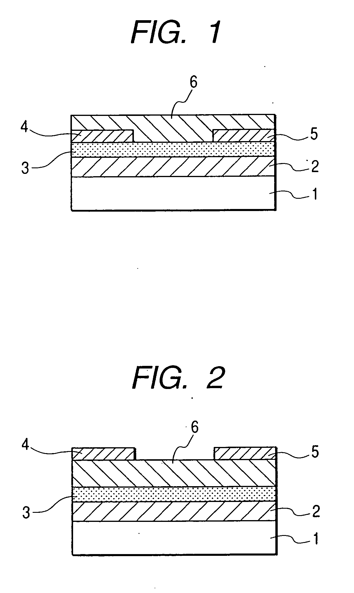
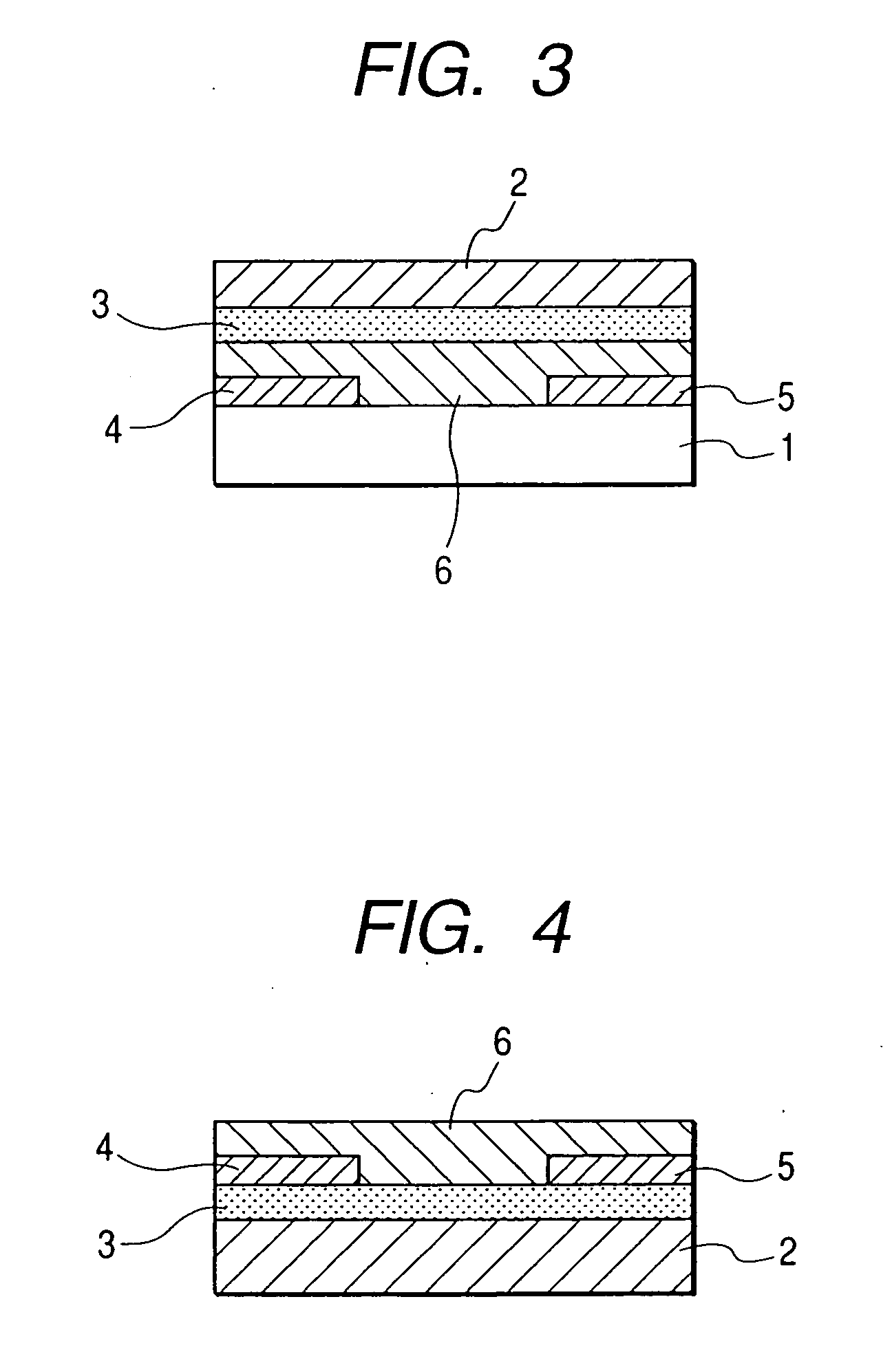
[0053]FIG. 4 shows the structure of a bottom gate type field effect transistor in this example.
[0054] First, a highly doped N-type silicon substrate was provided as the gate electrode 2. A silicon oxide film of 5,000 Å in thickness obtained by thermal oxidation of the silicon substrate surface layer was provided as the gate insulating layer 3. Chromium and gold were deposited from the vapor in this order onto the gate insulating layer 3 to form the source electrode 4 and the drain electrode 5 by means of an ordinary photolithography technique. Subsequently, the substrate surface was treated with ozone. Then, a coating film made from a 1 wt % chloroform solution of the bicycloporphyrin copper complex synthesized in Synthesis Example 1 was formed on the substrate by means of a spin coating method. Furthermore, the substrate was heated on a hot plate at 220° C. to form the organic semiconductor layer 6 composed of a benzo compound represented by the following structural formula (7). I...
example 2
[0060] Operations similar to those of Example 1 were performed except that the channel length L and the channel width W were changed to 50 μm and 2 mm, respectively. Table 1 shows the results.
PUM
 Abstract
Description
Claims
Application Information