Method for forming insulation film

Inactive Publication Date: 2006-11-16
ASM JAPAN
View PDF14 Cites 26 Cited by
  • Summary
  • Abstract
  • Description
  • Claims
  • Application Information

AI Technical Summary

Benefits of technology

[0023] One aspect of this invention may involve a method for forming an insulation film on a semiconductor substrate by using a plasma CVD apparatus including a reaction chamber, which method comprises a step of directly vaporizing a silicon-containing hydrocarbon compound expressed by the general formula SiαOβCxHy (α, β, x, and y are integers) or SiαOβHpNq (α, β, and p are integers, q is an integer of 0-2) and then introducing it to the reaction chamber of the plasma CVD apparatus, a step of introducing an additive gas, the flow volume of which is substantially

Problems solved by technology

In these multi-layered structures, however, capacitance among individual wires hinders high speed operations.
First, the fluorinated amorphous carbon film has lower thermal stability (370° C.
), poor adhesion with silicon-containing materials and also lower mechanical strength.
The lower thermal stability leads to damage under high temperatures such as over 400° C. Poor adhesion may cause the film to peel off easily.
Further, the lower mechanical strength can jeopardize wiring materials.
As a result, the relative dielectric constant of the film cannot be reduced to a desired degree.
As a result, the source gas cannot stay in the reaction chamber for a sufficient length of time to cause po

Method used


Image

  • Method for forming insulation film
  • Method for forming insulation film
  • Method for forming insulation film

Examples


Example

EXAMPLE

[0101] Experiments were conducted as described below. The results are indicated in tables below. In these experiments, an ordinary plasma CVD device (EAGLE®-10, ASM Japan K.K.) was used as an experimental device wherein:

[0102] rw (radius of the silicon substrate): 0.1 m

[0103] d (space between the silicon substrate and the upper electrode): 0.024 m or 0.020 m

[0104] Ps (standard atmospheric pressure): 1.01×10⁵ Pa

[0105] Ts (standard temperature): 273 K

[0106] The thickness of each insulation film was set at 50 nm, except that the thickness of each insulation film for measuring a dielectric constant was set at 200 nm.

[0107] An insulation film was formed on a concave-convex surface of aluminum which had an aspect ratio of ⅓ to 1 / 10. Filling property of the film was evaluated by observing a cross section of the interconnect structure with a scanning electron microscope.

Example

Example 1 (Comparative Example)

[0108] An insulation film was formed on a substrate using a plasma CVD apparatus shown in FIG. 1 under the following conditions, and the resultant thin film had the following properties: [0109] Susceptor temperature: 400° C. [0110] DM-DEOS (dimethyldiethoxysilane) flow rate: 100 sccm [0111] He flow rate: 70 sccm [0112] 27 MHz RF applied: 1600 W [0113] Reactor pressure: 600 Pa [0114] Dielectric constant: 2.9 [0115] Modulus: 20 GPa [0116] Film stress: 40 MPa (tensile) [0117] Space between the silicon substrate and the upper electrode: 0.024 m [0118] Residence time: 320 msec.

[0119] The thin film formed on the substrate was then cured using a curing apparatus shown in FIG. 2 under the following conditions, and the cured film had the following properties: [0120] UV curing process: Wavelength: 172 nm, 3-10 mW / cm2, Susceptor temperature: 300° C., N2: 5 SLM, Pressure: 45 Torr, Time: 70 sec. [0121] Dielectric constant: 3.0 [0122] Film shrinkage: 5.3% [0123] M...

Example

Example 2

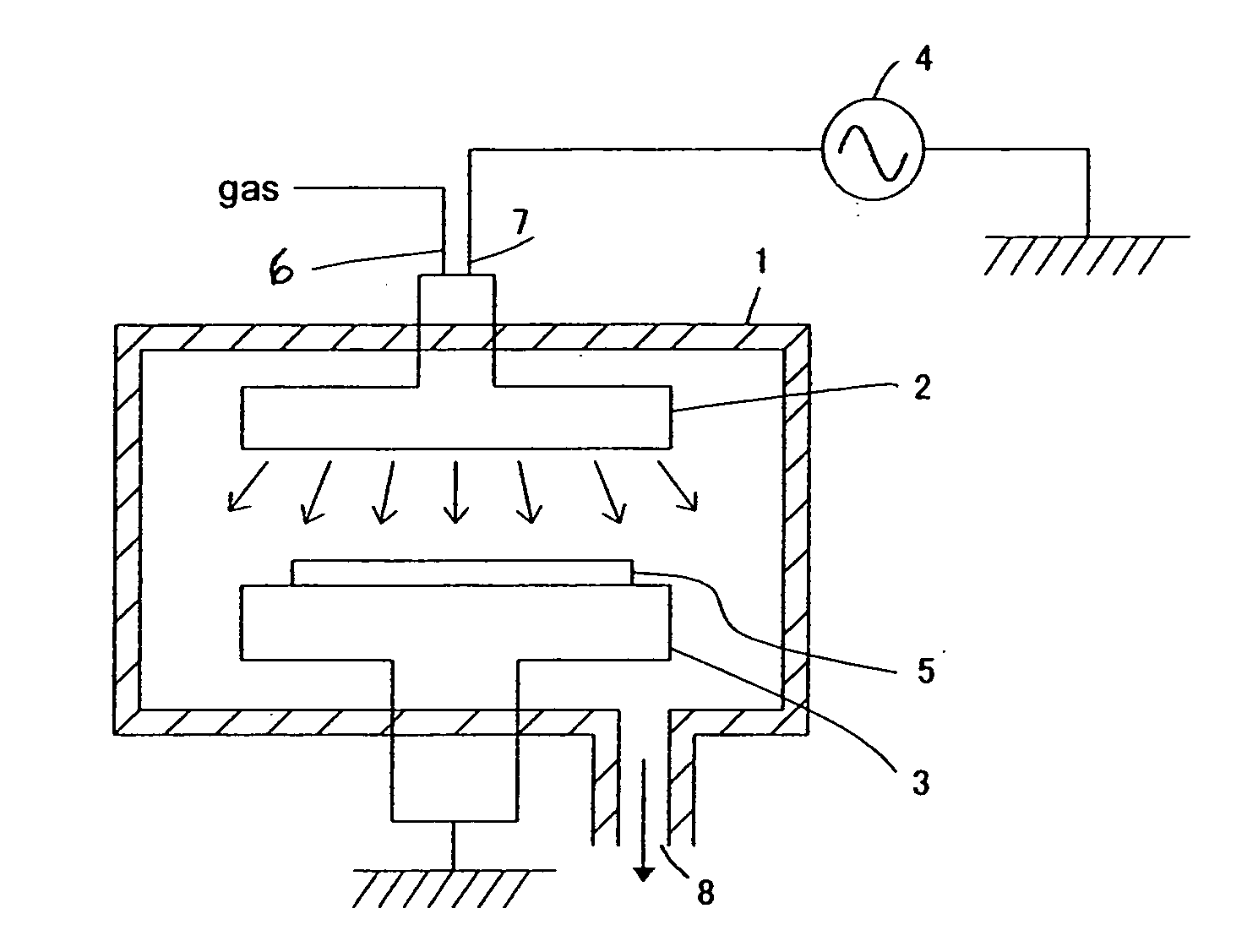
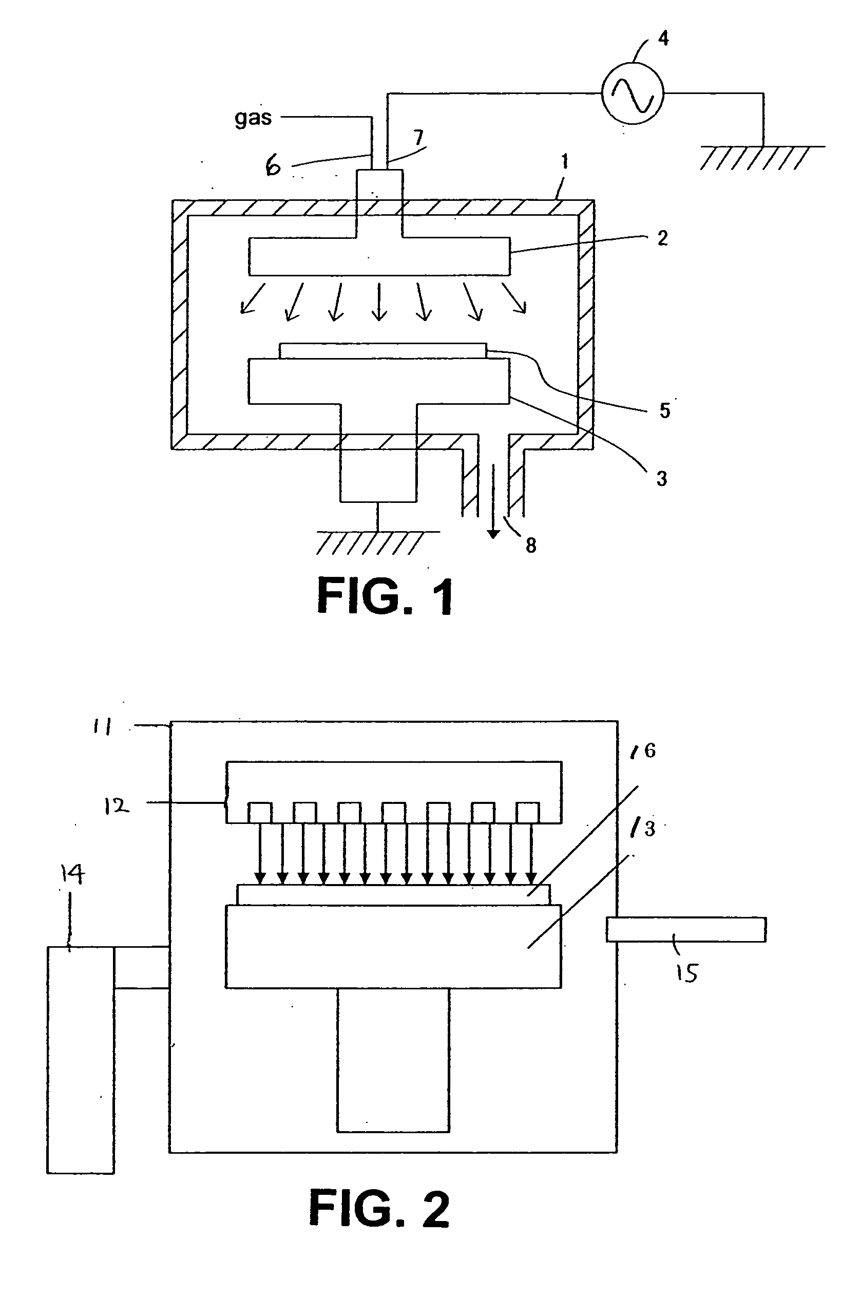
[0126] An insulation film was formed on a substrate using a plasma CVD apparatus shown in FIG. 1 under the following conditions, and the resultant thin film had the following properties:

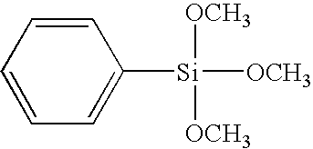
[0127] Susceptor temperature: 10° C. [0128] DM-DEOS (dimethyldiethoxysilane) flow rate: 10 sccm [0129] He flow rate: 650 sccm [0130] O2 flow rate: 500 sccm [0131] Isopropyl alcohol flow rate: 150 sccm [0132] 27 MHz RF applied: 250 W [0133] Reactor pressure: 666 Pa [0134] Space between the silicon substrate and the upper electrode: 0.024 m [0135] Residence time: 118 msec.

[0136] The thin film formed on the substrate was then annealed under the following conditions, and the annealed film had the following properties: [0137] Annealing process: Susceptor temperature: 450° C., N2: 3 SLM, Pressure: 800 Pa, Time: 600 sec. [0138] Dielectric constant: 2.7 [0139] Film shrinkage: 10.3% [0140] Modulus: 6 GPa [0141] Film stress: 55 MPa (tensile) [0142] Filling property (Padding property): Voids were no...


PUM

PropertyMeasurementUnit
Temperatureaaaaaaaaaa

Abstract

A method for forming an insulation film having filling property on a semiconductor substrate by plasma reaction includes: vaporizing a silicon-containing hydrocarbon having a Si—O bond compound to provide a source gas; introducing the source gas and a carrier gas without an oxidizing gas into a reaction space for plasma CVD processing; and forming an insulation film constituted by Si, O, H, and optionally C or N on a substrate by plasma reaction using a combination of low-frequency RF power and high-frequency RF power in the reaction space. The plasma reaction is activated while controlling the flow of the reaction gas to lengthen a residence time, Rt, of the reaction gas in the reaction space.

Description

BACKGROUND OF THE INVENTION [0001] This is a continuation-in-part of U.S. patent application Ser. No. 11 / 294,319, which is a continuation-in-part of U.S. patent application Ser. No. 10 / 412,363 filed Apr. 11, 2003, which is a continuation-in-part of U.S. patent application Ser. No. 10 / 317,239 filed Dec. 11, 2002, now U.S. Pat. No. 6,881,683, which is a continuation-in-part of U.S. patent application Ser. No. 09 / 827,616 filed Apr. 6, 2001, now U.S. Pat. No. 6,514,880, which is a continuation-in-part of (i) U.S. patent application Ser. No. 09 / 243,156 filed Feb. 2, 1999, now abandoned, which claims priority to Japanese patent application No. 37929 / 1998 filed Feb. 5, 1998, (ii) U.S. application Ser. No. 09 / 326,847 filed Jun. 7, 1999, now U.S. Pat. No. 6,352,945, (iii) U.S. patent application Ser. No. 09 / 326,848 filed Jun. 7, 1999, now U.S. Pat. No. 6,383,955, and (iv) U.S. patent application Ser. No. 09 / 691,376 filed Oct. 18, 2000, now U.S. Pat. No. 6,432,846, all of which are incorporat...

Claims


Application Information

Patent Timeline
IPC IPC(8): H01L21/31
CPCB05D1/62C09D4/00H01L2924/0002H01L2924/12044H01L23/296C23C16/30C23C16/401H01L21/02164H01L21/02214H01L21/02274H01L21/02348H01L21/3121H01L21/3122H01L21/31612C08G77/00H01L2924/00
Inventor FUKAZAWA, ATSUKIMATSUKI, NOBUOUMEMOTO, SEIJIRO
Owner ASM JAPAN
Why Eureka
Try Eureka