Linear semiconductor substrate, and device, device array and module, using the same

Inactive Publication Date: 2006-11-23
FURUKAWA ELECTRIC CO LTD
View PDF4 Cites 17 Cited by
  • Summary
  • Abstract
  • Description
  • Claims
  • Application Information

AI Technical Summary

Benefits of technology

[0117] According to the present invention, there is introduced a concept of a linear substrate into a field of semiconductor substrate for the first time, it becomes possible to decrease a thickness of a semiconductor layer down to a required minimum, to thereby drastically decrease a raw material cost of the semiconductor substrate. Further, high melting point backings such as quartz glass or the like are each used as the linear substrate to thereby enable usage of a thermal process in an ordinary pressure state or pressurized state, to realize fabricating of linear semiconductor substrates simultaneously in a high speed manner and a mass-production manner, thereby allowing for a decreased fabricating cost. Furthermore, the linear semiconductor substrates are each made to have a cross section in a rectangular shape, polygonal shape or the like, thereby enabling a plurality of faces of each linear semiconductor substrate to be sterically formed with devices, circuits, and/or wi

Problems solved by technology

As a result, upsizing a screen considerably deteriorates a yield, when a defect occurrence ratio is unchanged.
This naturally leads to an increased fabricating cost per one display, thereby problematically and considerably increasing a fabricating cost in inverse proportion to the yield.
This is because, when even one portion of a screen has a defective device, it is

Method used


Image

  • Linear semiconductor substrate, and device, device array and module, using the same
  • Linear semiconductor substrate, and device, device array and module, using the same
  • Linear semiconductor substrate, and device, device array and module, using the same

Examples


first embodiment

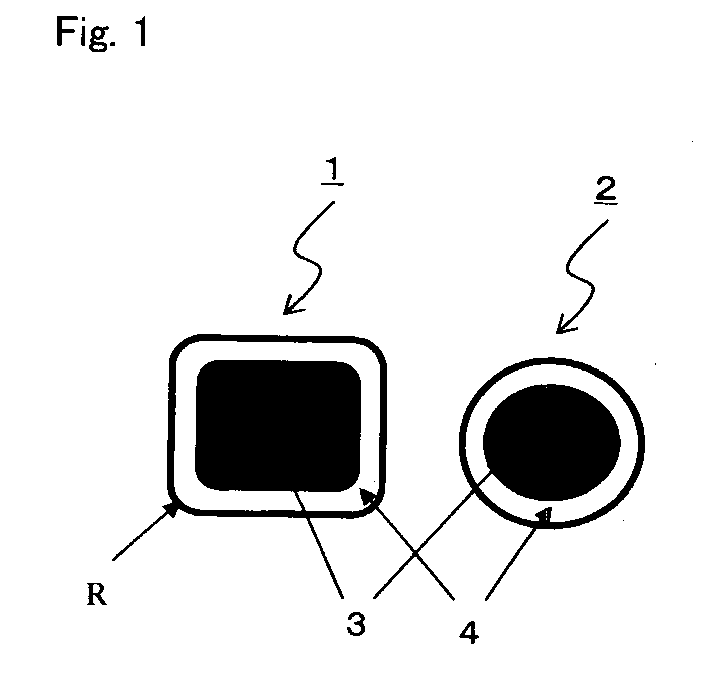
[0201] There will be firstly explained a linear substrate according to a first embodiment, with reference to the drawings. FIG. 1 is a cross-sectional view of linear substrates according to the first embodiment. The linear substrates of the present invention each comprises at least one desired thin film formed on or around a linear substrate having a length ten or more times greater than a width, thickness, or diameter of the linear substrate itself. Although FIG. 1 shows only cross sections of the linear substrates, the linear substrates of the present invention each have a sufficient length more than ten times greater than a width, thickness, or diameter of the illustrated cross section.

[0202] In the first embodiment, there will be described a linear semiconductor substrate to be used as a semiconductor substrate, among linear substrates. FIG. 1 shows linear semiconductor substrates 1 and 2 each comprising a polycrystalline silicon (p-Si) 4 as a semiconductor thin film deposited ...

second embodiment

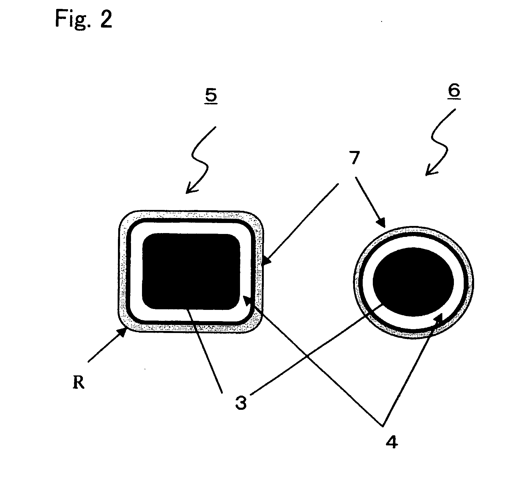
[0210]FIG. 2 is a cross-sectional view of linear semiconductor substrates according to a second embodiment. The second embodiment embraces linear semiconductor substrates 5 and 6 comprising the linear semiconductor substrates 1 and 2 of the first embodiments, respectively, as well as additional thin films 7 formed thereon, respectively. Each thin film 7 is provided by depositing an oxide film, thermally-oxidized film, nitride film, or the like in a range of several nanometers to 100 nm, so as to protect the associated polycrystalline silicon 4 inside it. Examples of the thin film 7 include SiO2, Si3N4, and the like. Such SiO2 comprises a thermally-oxidized film or is formed by a thermal CVD method.

third embodiment

[0211]FIG. 3 shows a cross-sectional view of linear semiconductor substrates according to a third embodiment. The third embodiment embraces linear semiconductor substrates 8 and 9 each comprising a quartz glass backing 3, a semiconductor thin film of polycrystalline silicon 10 deposited on a surface of the quartz glass backing 3, and another semiconductor thin film of polycrystalline silicon 11 formed on the semiconductor thin film of polycrystalline silicon 10. The polycrystalline silicon 10 as the first semiconductor thin film is doped with boron (B), aluminum (Al), or the like as a P type dopant, while the polycrystalline silicon 11 as the second semiconductor thin film is doped with phosphorus (P), bismuth (Bi), or the like as an N type dopant. The linear semiconductor substrates of the present invention can be each adopted as a substrate for a solar cell, and there was obtained a conversion efficiency of 12% to 15% when the polycrystalline silicon 10 thin film as the first semi...


PUM

PropertyMeasurementUnit
Temperatureaaaaaaaaaa

Abstract

The linear semiconductor substrate 1 or 2 of the present invention comprises at least one desired thin film 4 formed on a linear substrate 3 having a length ten or more times greater than a width, thickness, or diameter of the linear substrate itself. Adopting semiconductor as the thin film 4 forms a linear semiconductor thin film. The linear semiconductor substrate 1 or 2 of the present invention is produced by utilizing a fiber-drawing technique which is a fabricating technique of optical fibers.

Description

TECHNICAL FIELD [0001] The present invention relates to a linear or one-dimensional semiconductor substrate as a semiconductor circuit substrate and a fabricating method thereof, and a device, a device array, a module, a display, a solar cell, a solar cell module using the linear semiconductor substrate, and a fabricating method thereof. BACKGROUND ART [0002] Generally, substrates to be typically used, such as semiconductor substrates exemplarily made of silicon, gallium arsenide (GaAs), gallium nitride (GaN) and the like, and a glass substrate for display, are two-dimensional planar substrates, respectively. [0003] The semiconductor substrates such as made of silicon, GaAs, and the like are each provided and used in a manner to pull up a molten raw material by using a seed crystal to thereby fabricate an ingot of single crystal, and to cut it into semiconductor substrates, followed by application of grinding and polishing to provide them with mirror surfaces, respectively. [0004] I...

Claims


Application Information

Patent Timeline
IPC IPC(8): H01L21/00H01L33/00H01L29/06H01L31/0352
CPCB82Y10/00C23C16/44C23C16/545H01L27/304H01L29/0657Y10T428/2933H01L29/0673H01L31/0352H01L31/035281Y02E10/50H01L31/0475H01L29/0665H10K30/53
Inventor NAKAMURA, TOSHIHIROORITA, NOBUAKIKOAIZAWA, HISASHISUZUKI, KENKICHIKURASEKO, HIROSHIKONDO
Owner FURUKAWA ELECTRIC CO LTD
Why Eureka
Try Eureka