

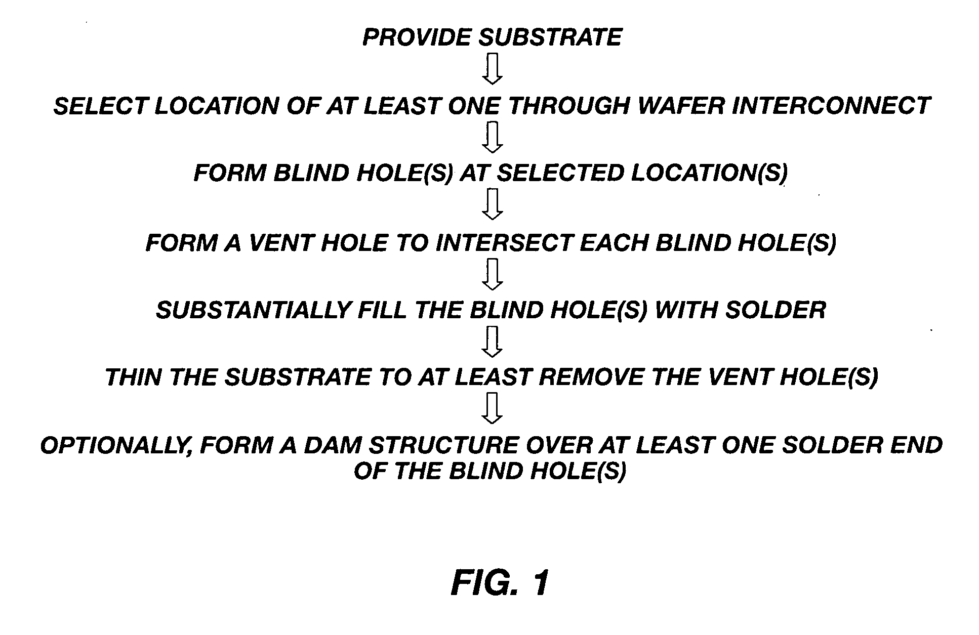
Methods for forming through-wafer interconnects, intermediate structures so formed, and devices and systems having at least one solder dam structure
a technology of through-wafer interconnection and intermediate structure, which is applied in the direction of semiconductor devices, semiconductor/solid-state device details, electrical apparatus, etc., can solve the problems of molten solder being wicked into the hollow, molten solder being buried in the hollow, and depleting the ball of sufficient solder to complete the conductive connection
- Summary
- Abstract
- Description
- Claims
- Application Information
AI Technical Summary
Benefits of technology
Problems solved by technology
Method used
Image

Examples
Embodiment Construction
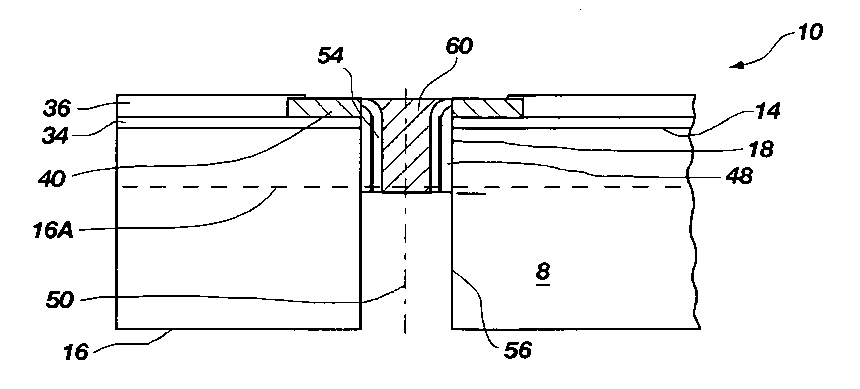
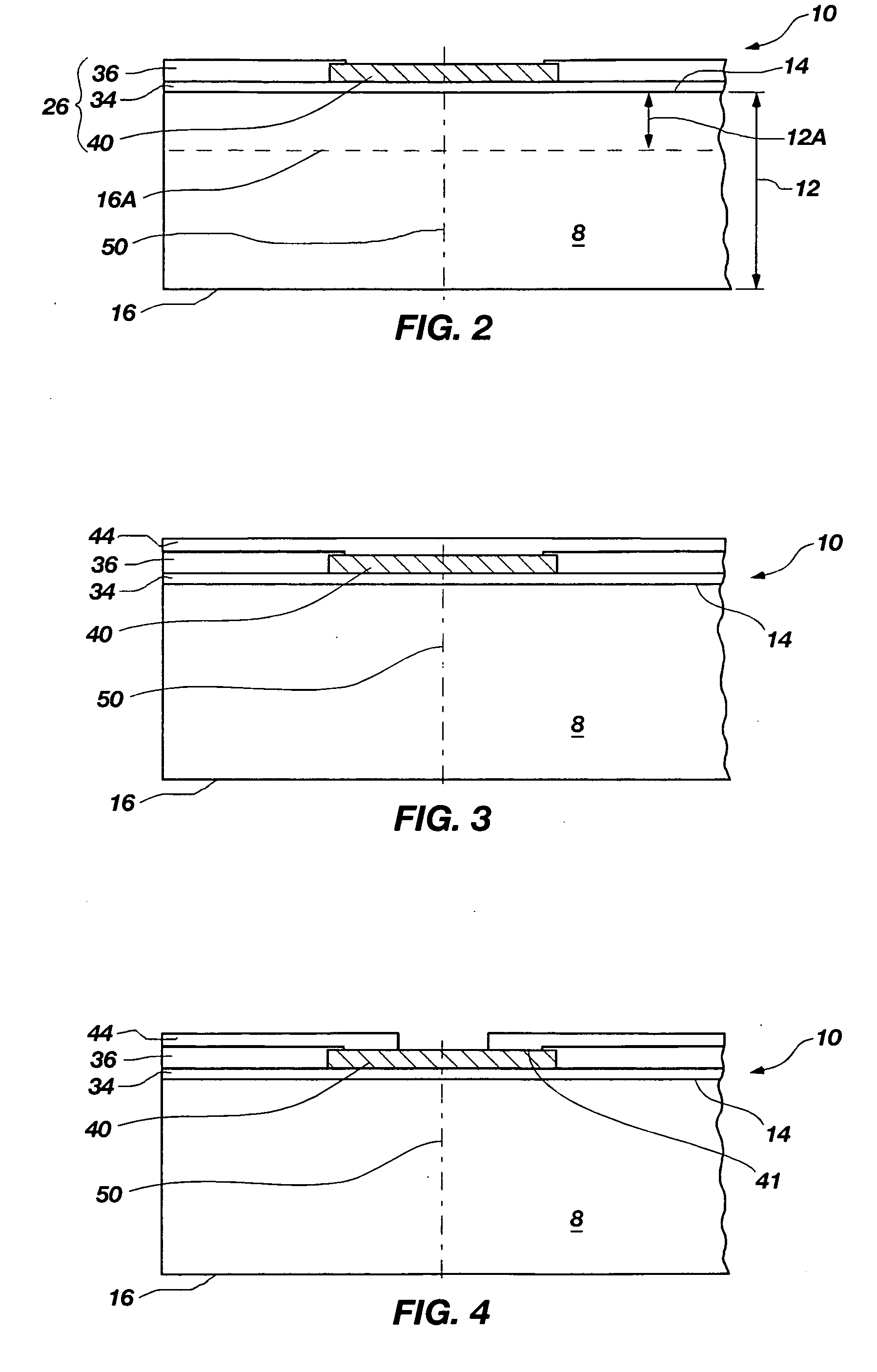
[0043] The invention comprises methods for forming through vias (“TV”) or through-wafer interconnects (“TWIs”) through a substrate structures. The term “via” is a general term denoting a conductor passing through a substrate structure. The term “through-wafer interconnect” is often used more specifically where the substrate structure is a wafer of semiconductor material (e.g., a semiconductor wafer). In this application, the terms “substrate” and “wafer” will be used interchangeably as encompassing any substrate material which may be subjected to a thinning process for reducing its thickness. Thus, the methods of the present invention relate to semiconductor devices whether in the wafer form or individualized die form that are thinnable to a final thickness. Accordingly, the term “substrate” refers not only to silicon wafers (e.g., monocrystalline silicon or polycrystalline silicon) but may also refer to silicon on insulator (“SOI”) substrates, silicon on sapphire (“SOS”) substrates...
PUM
 Abstract
Description
Claims
Application Information