Deposition of perovskite and other compound ceramic films for dielectric applications

a technology of compound ceramic films and perovskite, which is applied in the direction of fixed capacitor details, fixed capacitors, natural mineral layered products, etc., can solve the problems of limited materials that can be used in device manufacture, limited materials that can be utilized as substrates, and limited materials. the effect of specific capacitan

Inactive Publication Date: 2007-03-08
DEMARAY
View PDF99 Cites 54 Cited by
  • Summary
  • Abstract
  • Description
  • Claims
  • Application Information

AI Technical Summary

Benefits of technology

[0006] In accordance with the present invention, deposition of layers in a pulsed-DC physical vapor deposition process from a conductive ceramic target is presented. In some embodiments, the deposition can provide a low-temperature, high deposition-rate deposition of a dense amorphous layer of BST from a conductive BST target, which can be annealed at much lower temperature to yield crystalline BST. Some embodiments of the deposition address the need for low temperature, high rate deposition of perovskite films, for example BST films, which can be utilized as the dielectric layer in high specific capacitance devices as, for example, de-coupling capacitors, energy storage devices, voltage tunable capacitors, or other micro-electronic devices.

Problems solved by technology

For all of the potential, thin film perovskites have rarely been utilized in manufacture primarily because of difficulties in controlling physical and chemical properties of the crystalline and amorphous phases of perovskite thin-film materials and their interactions with metallic and conductive electrodes.
However, conventional materials and production processes can limit the types of materials that can be used in device manufacture.
Such a high temperature anneal, however, severely limits the materials that can be utilized as the substrate, and often requires the use of expensive noble metals such as platinum to protect the substrate from reaction with the electrode material.
Such high heat-treat temperatures are incompatible with standard semiconductor or MEM device processing, and limit the choice of substrate materials on which the layers can be formed, increasing the cost, and decreasing the yield of such devices formed with the layers.

Method used


Image

  • Deposition of perovskite and other compound ceramic films for dielectric applications
  • Deposition of perovskite and other compound ceramic films for dielectric applications
  • Deposition of perovskite and other compound ceramic films for dielectric applications

Examples


Embodiment Construction

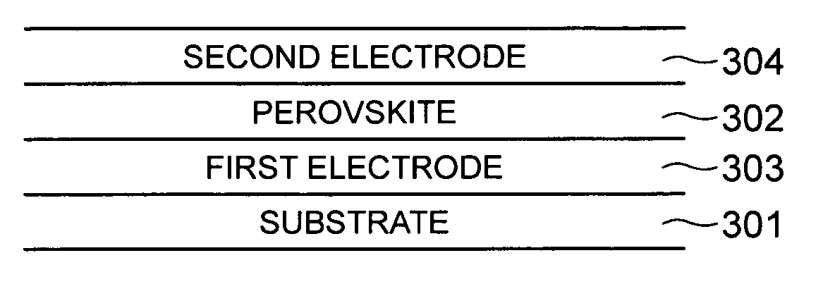
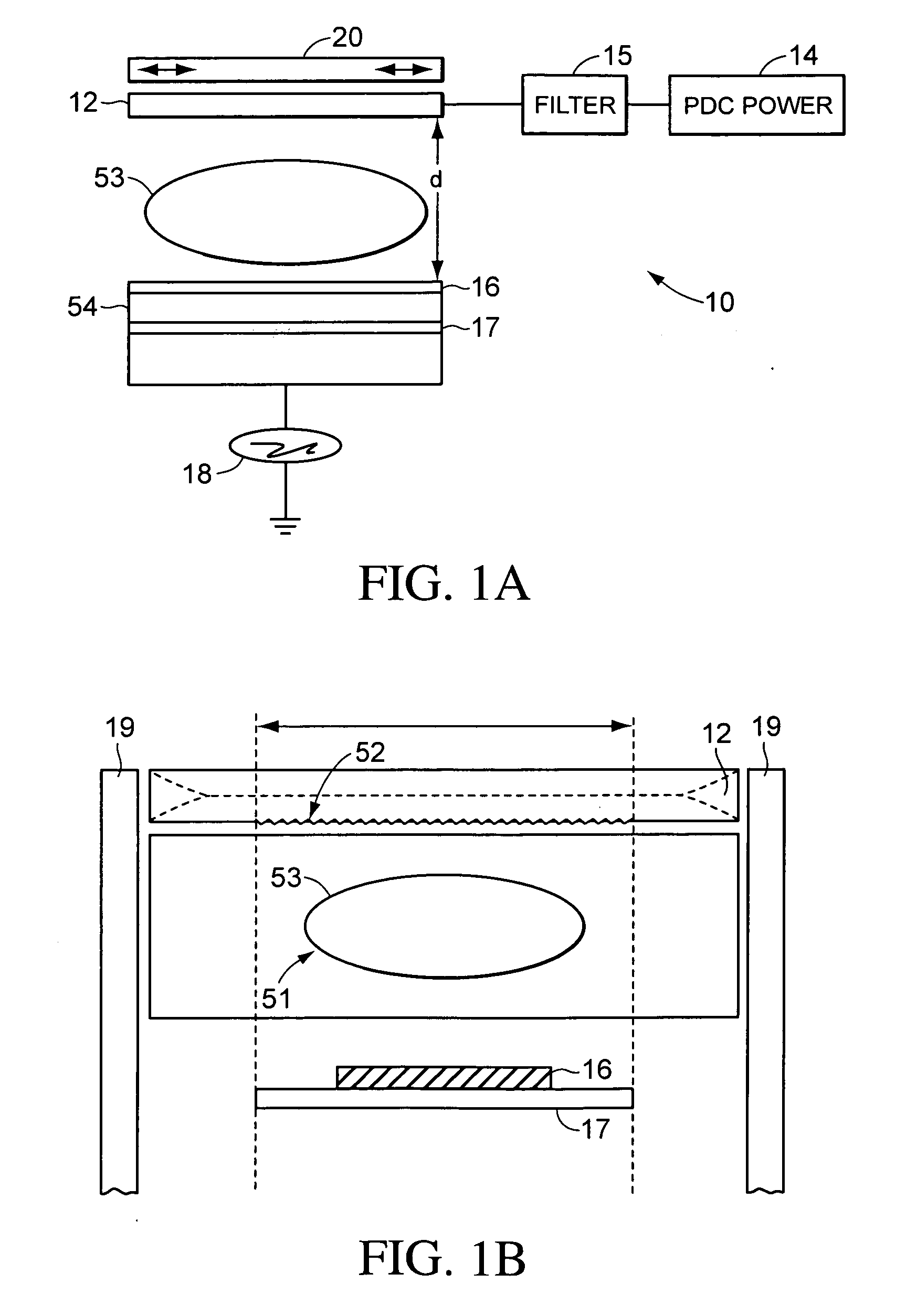
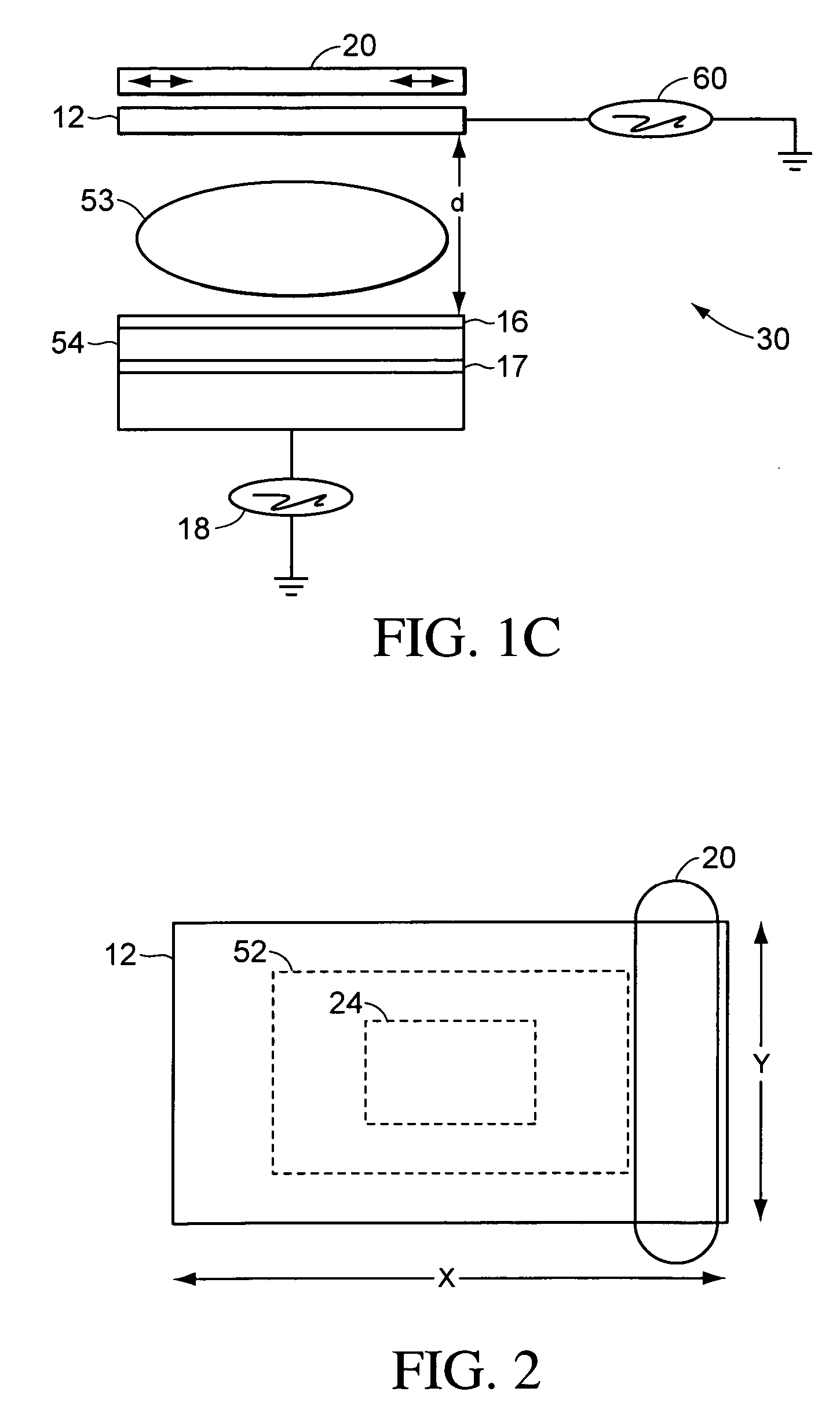
[0025] In accordance with embodiments of the present invention, dielectric perovskite films or other ceramic oxide films are deposited on a substrate by a pulsed-DC physical vapor deposition (PVD) process utilizing a conductive ceramic target. In some embodiments, the film can be deposited by RF sputtering.

[0026] In some embodiments, a dielectric perovskite layer, for example BST material, is deposited directly on the substrate with only low temperature anneal, eliminating the need of a subsequent high temperature anneal to crystallize the film. Removing the high temperature anneal allows for formation of capacitor structures on light-weight, low temperature, and low cost substrates such as copper foil and plastic sheet, reducing both the weight and the cost of capacitors while maintaining the high dielectric constant of the perovskite, for example BST, high-density dielectric film.

[0027] Deposition of materials by pulsed-DC, RF biased reactive ion deposition is described in U.S. ...


PUM

PropertyMeasurementUnit
thickaaaaaaaaaa
thickaaaaaaaaaa
temperatureaaaaaaaaaa

Abstract

In accordance with the present invention, deposition of perovskite material, for example barium strontium titanite (BST) film, by a pulsed-dc physical vapor deposition process or by an RF sputtering process is presented. Such a deposition can provide a high deposition rate deposition of a layer of perovskite. Some embodiments of the deposition address the need for high rate deposition of perovskite films, which can be utilized as a dielectric layer in capacitors, other energy storing devices and micro-electronic applications. Embodiments of the process according to the present invention can eliminate the high temperature (>700° C.) anneal step that is conventionally needed to crystallize the BST layer.

Description

FIELD OF THE INVENTION [0001] The present invention is related to production and application of dielectric thin-films and, in particular, the deposition of perovskites such as Barium Strontium Titanate (BST) films and other ceramic oxides for dielectric applications. DISCUSSION OF RELATED ART [0002] Perovskite films, for example Barium Strontium Titanate (BST) films, are one of the attractive materials to use in capacitors for high density device applications because of its relatively high dielectric constant, low leakage current density, high dielectric breakdown strength, and ferroelectric perovskite phase that does not exhibit fatigue. However, electric properties of the perovskite films are greatly dependent on the deposition process, the substrate, the post-processing, and the related film structure. For all of the potential, thin film perovskites have rarely been utilized in manufacture primarily because of difficulties in controlling physical and chemical properties of the cr...

Claims


Application Information

Patent Timeline
Patent Type & Authority Applications(United States)
IPC IPC(8): H01G4/06
CPCC23C14/088C23C14/3414C23C14/345H01L21/31691H01G4/1227H01G4/30C23C14/50H01G4/33H01G4/085H01L21/02266H01L21/02197
Inventor ZHANG, HONGMEIDEMARAY, RICHARD E.
Owner DEMARAY
Why Eureka
Try Eureka