

Gate turn-off thyristor
a technology of thyristor and turn-off thyristor, which is applied in the direction of basic electric elements, electrical apparatus, and semiconductor devices, can solve the problems of crystal defects, high cost, and high cost, and achieve low cost, low resistance, and relatively high resistance.
- Summary
- Abstract
- Description
- Claims
- Application Information
AI Technical Summary
Benefits of technology
Problems solved by technology
Method used
Image

Examples
first embodiment
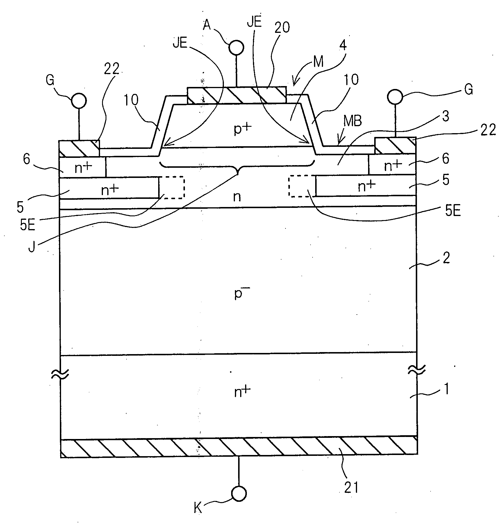
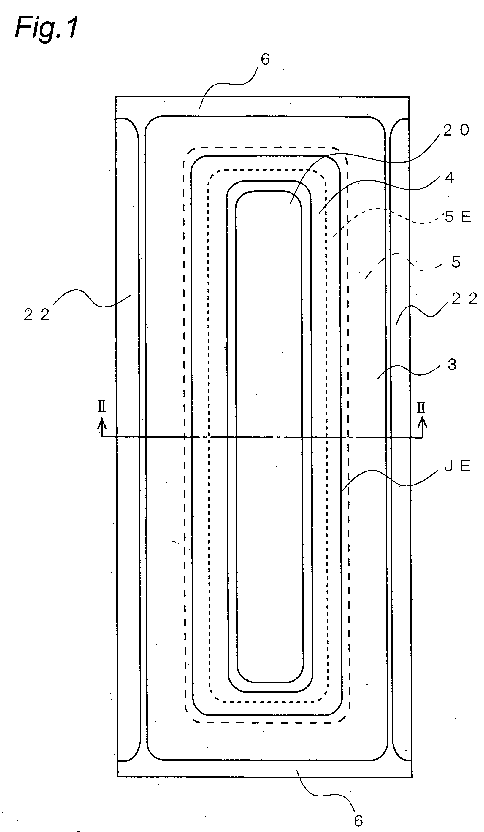
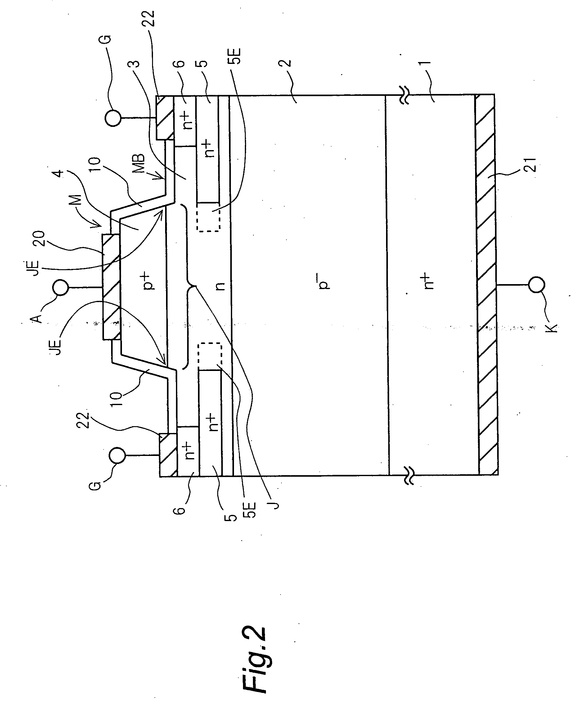
[0042] A GTO that uses SiC of the first embodiment of the present invention is described with reference to FIGS. 1 and 2. FIG. 1 is a top view that shows the upper surface before the provision of an insulator 10 of the GTO of the first embodiment. FIG. 2 is a sectional view taken along the line II-II of FIG. 1. In FIGS. 1 and 2, the GTO of the present embodiment has a heavily doped cathode emitter layer 1 (first emitter layer) of an n-type (first conductive type) SiC semiconductor that has a thickness of about 350 μm and an impurity concentration of not smaller than about 1019 cm−3 and is provided with a cathode electrode 21 (first electrode) connected to the cathode terminal K (cathode K, hereinafter). A lightly doped base layer 2 (first base layer) of a p-type (second conductive type) SiC semiconductor that has a thickness of 50 μm and an impurity concentration of about 1016 to 1013 cm−3 is formed on the cathode emitter layer 1. A thin n-type base layer 3 (second base layer) of a ...
second embodiment
[0051]FIG. 3 is a sectional view of a GTO that uses SiC of the second embodiment of the present invention. In FIG. 3, the p-type and the n-type of the layers are interchanged in the GTO of the present embodiment in comparison with the GTO of the first embodiment shown in FIG. 2. A lightly doped n-type SiC base layer 2 (second base layer) that has a thickness of about 50 μm is formed on the upper surface of a p-type anode emitter layer 4A (first emitter layer) that has a thickness of about 350 μm and is provided with an anode electrode 20 (first electrode) connected to the anode A on its lower surface. A thin p-type base layer 3A (second base layer) that has a thickness of several micrometers is formed on the base layer 2A, and an n-type layer of which central region is left in a subsequent process to serve as an n-type cathode emitter layer 1A is formed by the epitaxial growth method on the entire surface of the p-type base layer 3A. Next, a region is deeply etched by the reactive i...
third embodiment
[0054]FIG. 4 is a sectional view of a GTO that uses SiC of the third embodiment of the present invention. In the GTO of the present embodiment shown in the figure, a p-type region 7, which includes at least the neighborhood of the end portion of the junction J between the p-type anode emitter layer 4 and the n-type base layer 3 and expands from the neighborhood of a corner portion MC of the mesa M toward the gate electrode 22, is formed in the n-type base layer 3. The other construction is the same as that of the GTO of the first embodiment shown in FIG. 2. By virtue of the formation of the p-type region 7, the field intensity of the insulator 10 in the neighborhood of the mesa corner portion MC located at the end portion of the junction J between the p-type anode emitter layer 4 and the n-type base layer 3 can be relieved even when the off-gate voltage at the turn-off time is increased. As a result, the withstand voltage between the gate G and the anode A can be raised, and the con...
PUM
 Abstract
Description
Claims
Application Information