

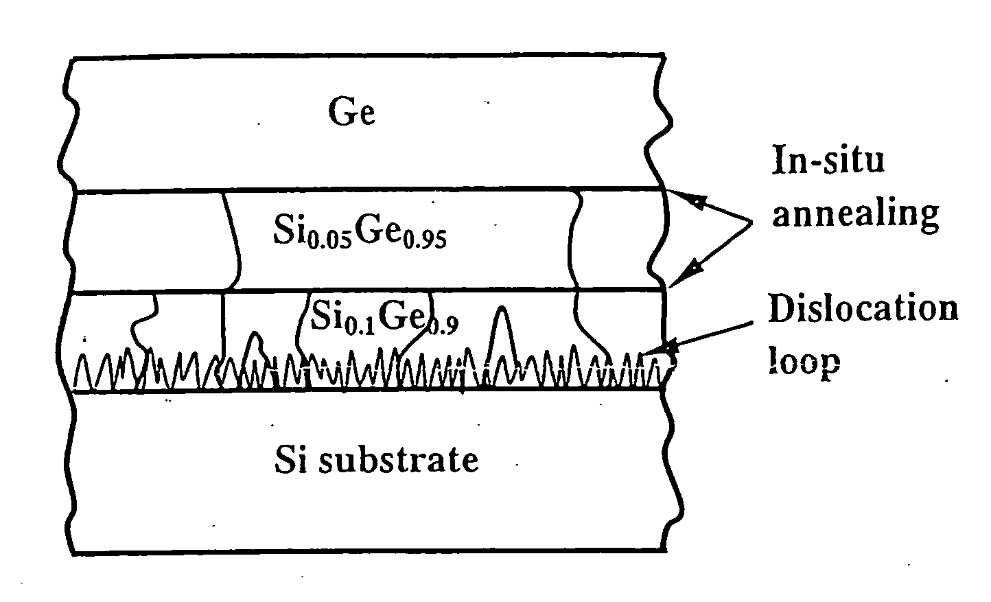
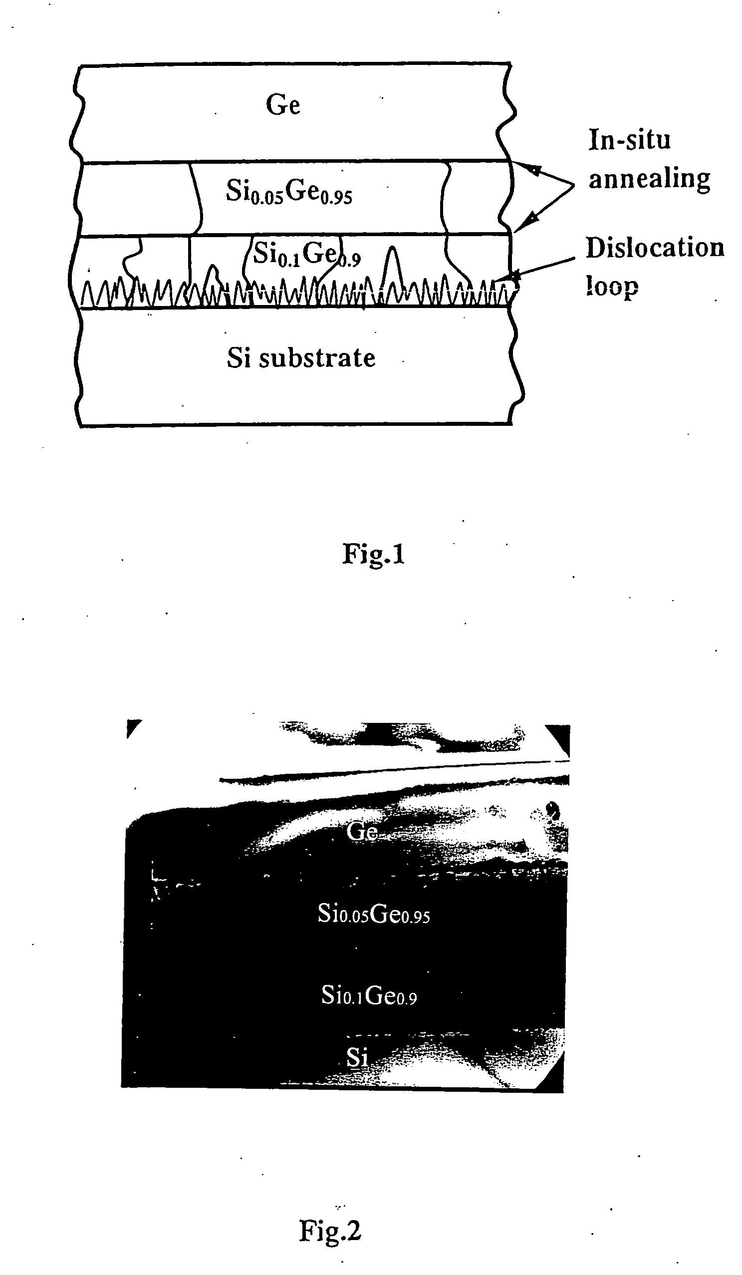
Growth of GaAs expitaxial layers on Si substrate by using a novel GeSi buffer layer
a technology of gesi and gaas, which is applied in the direction of semiconductor devices, electrical equipment, basic electric elements, etc., can solve the problems of high density threading, network of misfit dislocation, and device structure based on heteroepitaixial gaas on silicon with a 4.0% difference in lattice constant and additional intrinsic thermal conductivity difference, etc., to achieve flattening surface roughness, reducing high defect density, and reducing the thickness of ge epi
- Summary
- Abstract
- Description
- Claims
- Application Information
AI Technical Summary
Benefits of technology
Problems solved by technology
Method used
Image

Examples
Embodiment Construction
[0029] The invention will be now illustrated in the following example but not be limited to.
[0030] Firstly, pre-cleaning the silicon wafer in a standard cleaning procedure, wherein the cleaning treatment comprises steps of boiling the silicon wafer in a solution containing the mixtures of H2O2:H2SO4 with the ratio 1:4 in about 10 min., then taking and rinsing it with de-ion water in 10 min., furthermore dipping it in a solution of 10% HF in 30 seconds and subsequently further taking and rinsing it into de-ion water loading the wafer into a UHVCVD system immediately after said cleaning and prebaking the wafer at 850° C. in 10 min to remove the native oxided layer and then cooling the temperature of UHVCVD system down to 400° C. While temperature of system present stable and is capable of growing a high Ge-composition SiGe epitaixial layer. Wherein UHVCVD system is a quartz tube furnace equipped with heating sources, and the background is vacuumed by a molecular pump to a pressure of...
PUM
| Property | Measurement | Unit |
|---|---|---|
| thickness | aaaaa | aaaaa |
| thickness | aaaaa | aaaaa |
| thickness | aaaaa | aaaaa |
Abstract
Description
Claims
Application Information