Resin Composition and Semiconductor Device Produced By Using the Same

a technology of composition and semiconductor, which is applied in the direction of conductive materials, solid-state devices, non-conductive materials with dispersed conductive materials, etc., can solve the problems of high temperature conductive adhesive, thermal management, and release of heat from semiconductor products, etc., to achieve excellent adhesion, short curing time, and quick curability

Inactive Publication Date: 2007-09-13
SUMITOMO BAKELITE CO LTD
View PDF12 Cites 9 Cited by
  • Summary
  • Abstract
  • Description
  • Claims
  • Application Information

AI Technical Summary

Benefits of technology

[0031] A resin composition of the present invention, particularly a resin composition which belongs to any of the above-mentioned first to sixth composition systems, is excellent in adhesion strength, quick curability, moisture resistance and low stress property, is also applicable to the oven curing, and is excellent in adhesion particularly between a copper lead frame and a semiconductor chip when it is used as an adhesive of a semiconductor chip. Also, the obtained semiconductor device is excellent in solder crack resistance. As a result, a semiconductor device which is high in reliability can be obtained.
[0032] Also, among the resin compositions of the present invention, the composition which belongs to the third composition system exhibits excellent bleeding property as well as good low stress property and good adhesion, therefore, a semiconductor device excellent in reliability can be obtained by using the resin composition as a die attach material for a semiconductor or a bonding material for a heat dissipating member or an attach material for a heat sink member.

Problems solved by technology

Hence, in comparison with a curing condition of a die attach paste in the conventionally employed batch method, time required for curing is significantly limited.
In relation with the above requirements of shortening of curing time and lowering of curing temperature, there is another problem, which is a requirement of thermal management.
With significant increase in capacity and processing speed of semiconductor products and moving towards finer design rule, a problem of heat which generates during operation of semiconductor products is becoming prominent so that releasing the heat from semiconductor products, i.e. thermal management, is becoming an important issue.
However, a highly thermal conductive adhesive has some problems as follows (For example, see JP-A No. Hei. 11-43587).
However, since there is a limit in containing amount, there are cases that high thermal conductivity cannot be obtained.
Also, though the highly thermal conductive adhesive containing a large amount of solvent has a good thermal conductivity as a sole cured product, the state when it is applied to a semiconductor product may not have a stable thermal conductivity since the solvent remains in the cured product or the solvent volatilizes to leave voids.
Even if the adhesive could contain a large amount of thermally conductive particles, there are cases that low stress property is insufficient due to high containing rate of the thermally conductive particles.
Because the use of such a lead-free solder causes increase of stress due to raised reflow temperature, semiconductor products easily generate delamination and thus cracking during the reflow process.
However, such a roughened surface often causes resin bleeding of die attach paste which leads to serious problems such as decline in package reliability.
In relation to the above-mentioned problems, in case of epoxy resin type die attach paste, which is a major die attach paste at present, curing can be performed in about 60 seconds by using amine type curing agents or the like, however, curing in a very short time such as 15 to 30 seconds is not handled yet.
However, there are disadvantages that water absorption property of a cured product becomes high when an imide compound is used solely so as to deteriorate properties of a cured product after moisture absorption since imide compounds have high polarity.
There has not been any satisfactory compound particularly in view of adhesion to hardly adhesive surfaces such as Ni—Pd plated frames or the like, low stress property against increase of stress caused by raised reflow temperature due to the change to lead-free solder, and moisture resistance.
Also, a material which has better adhesion to Ni—Pd plated frames than conventionally used die attach pastes (for example, see JP-A No. 2000-273326), has excellent low stress property in terms of low elastic modulus, and does not generates resin bleeding is desired, however, there has not been satisfactory material.

Method used


Image

  • Resin Composition and Semiconductor Device Produced By Using the Same
  • Resin Composition and Semiconductor Device Produced By Using the Same
  • Resin Composition and Semiconductor Device Produced By Using the Same

Examples


examples

[0124] The following experimental examples further describe the above-mentioned first to sixth composition systems of the present invention.

[0125] Firstly, experimental examples of the first composition system (Experimental example series A) are hereinafter described. The compounding ratio is in “part by weight”.

examples a1

to A4, Comparative Examples A1 to A3

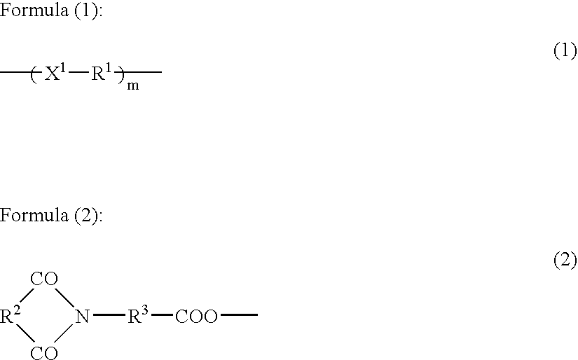
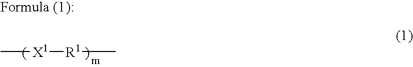
[0126] As the compound (B), polyether-based bismaleimide acetic ester (LUMICURE MIA-200, manufactured by DAINIPPON INK & CHEMICALS, INC., a compound wherein R2 is —C2H2— and R3 is —CH2— in the formula (2), and X1 is —O— and R1 is —C4H8— in the formula (1), hereafter referred as “compound 1”) was used. As the compound (D), polypropylene glycol dimethacrylate (BLEMMER PDP-400, manufactured by NOF Corporation, hereafter referred as “compound 2”) and polytetramethylene glycol dimethacrylate (BLEMMER PDT-800, manufactured by NOF Corporation, hereafter referred as “compound 3”) were used. As the thermal radical initiator (C), dicumyl peroxide (decomposition temperature: 126° C. in rapid heating test, Percumyl D, manufactured by NOF Corporation, hereafter referred as “initiator”) was used. As the filler (A), silver powder in a flake-like form having an average particle size of 3 μm and a maximum particle size of 20 μm (hereafter referred as “silver powde...

examples b1 to b4

, Comparative Examples B1 to B4

[0138] As the compound (B), polyether-based bismaleimide acetic ester (LUMICURE MIA-200, manufactured by DAINIPPON INK & CHEMICALS, INC., a compound wherein R2 is —C2H2— and R3 is —CH2— in the formula (2), and X1 is —O— and R1 is —C4H8— in the formula (1), hereafter referred as “compound 1”) was used. As the compound (D), polypropylene glycol dimethacrylate (BLEMMER PDP-400, manufactured by NOF Corporation, hereafter referred as “compound 2”) and polytetramethylene glycol dimethacrylate (BLEMMER PDT-800, manufactured by NOF Corporation, hereafter referred as “compound 3”) were used. As the compound (L) containing a glycidyl group, polytetramethylene glycol diglycidyl ether (ED-612, manufactured by Asahi Denka Co., Ltd., hereafter referred as “compound 4”) and polypropylene glycol diglycidyl ether (ED-506, manufactured by Asahi Denka Co., Ltd., hereafter referred as “compound 5”) were used. As the compound (M) which reacts with a glycidyl group, 2-pheny...


PUM

PropertyMeasurementUnit
timeaaaaaaaaaa
timeaaaaaaaaaa
timeaaaaaaaaaa

Abstract

A resin composition which is excellent in quick curing and can be used for curing in conventionally used ovens, and a semiconductor device which is excellent in reliability such as solder crack resistance or the like when the resin composition is used as a die attach material for semiconductor. Further preferably, a resin composition which has a sufficient low stress property, good adhesion and excellent bleeding property.
A resin composition comprising a filler (A), the compound (B) comprising a structure represented by the formula (1) and a functional group represented by the formula (2) and a thermal radical initiator (C), and substantially not containing a photo polymerization initiator.

Description

TECHNICAL FIELD [0001] The present invention relates to a resin composition and a semiconductor device using the same. BACKGROUND ART [0002] Aiming at improvement on productivity in a die-bonding process, in the production of semiconductors, the in-line curing method in which a die bonder, a wire bonder and the like are arranged on the same line is employed and it is tending to be more widely used from now on. Hence, in comparison with a curing condition of a die attach paste in the conventionally employed batch method, time required for curing is significantly limited. For example, with respect to the conventional oven curing method wherein curing is performed at 150 to 200° C. for 60 to 90 minutes, curing is required in a short time such as at 150 to 200° C. for 15 to 90 seconds in the case of the in-line curing method (for example, see Japanese Patent Application Laid-Open (JP-A) No. 2000-63452). [0003] With the enhancement of the processing speed of semiconductor devices, a chip...

Claims


Application Information

Patent Timeline
Patent Type & Authority Applications(United States)
IPC IPC(8): C08L23/04C08F290/06C08G69/40C08G69/46C09J201/02H01L21/52H01L21/58H01L23/373
CPCC08G73/12H01L23/145C08K5/0025C08K5/14C08L79/085C09J201/025H01L23/3737H01L24/83H01L2224/8385H01L2924/01004H01L2924/01005H01L2924/01009H01L2924/01013H01L2924/01015H01L2924/0102H01L2924/01027H01L2924/01029H01L2924/0103H01L2924/01033H01L2924/01046H01L2924/01047H01L2924/0105H01L2924/01057H01L2924/01077H01L2924/01078H01L2924/01079H01L2924/01082H01L2924/07802H01L2924/12044H01L2924/30105H01L24/29H01L2224/2919H01L2924/01006H01L2924/01019H01L2924/01024H01L2924/014H01L2924/0665C08K3/08H01L2924/10253C08K3/26C08F234/02C08F220/58H01L2224/29111C09J179/08H01L2924/1579H01L2924/15747H01L2924/0132H01L2924/00H01L2924/3512H01L2924/00015H01L2924/181C09J201/02C08F290/06H01L21/52
Inventor OKUBO, HIKARUTANAKA, NOBUKIWATANABE, ITARU
Owner SUMITOMO BAKELITE CO LTD
Why Eureka
Try Eureka