Methods of making a molecular detection chip having a metal oxide silicon field effect transistor on sidewalls of a micro-fluid channel

a technology of metal oxide silicon and field effect transistor, which is applied in the field of molecular detection chips, can solve the problems of difficult selective immobilization of biomolecular probes in a limited region, high integration of biosensors, and inability to detect high sensitivity binding to target molecules, etc., and achieves the effect of easy high integration

Inactive Publication Date: 2007-09-20
SAMSUNG ELECTRONICS CO LTD
View PDF37 Cites 23 Cited by
  • Summary
  • Abstract
  • Description
  • Claims
  • Application Information

AI Technical Summary

Benefits of technology

[0022] It is a first object of the present invention to provide a molecular detection chip that is easy to highly integrate and can detect the immobilization of probes and binding of a target molecule in situ within a short period of time.
[0027] It is a sixth object of the present invention to provide a new nucleic acid mutation assay device in which at least one thermal control and detection unit is formed in a micro-fluid channel by microfabrication so that DNA mutations can be detected in real time through accurate and precise temperature control.
[0039] The molecular detection chip and device according to the preset invention are advantageously easy to highly integrate and can detect immobilization of probes and coupling of a target molecule to the probes in situ.
[0047] It is preferable that the MOSFET is located at the sidewalls or convex corners of the micro-fluid channel. Unlike recently disclosed FET-based biomolecular sensors manufactured on a plain, a biomolecular sensor according to the present invention is formed as a 3-dimensional (3D) MOSFET sensor by bulk micromachining and diffusion and is disposed at the convex corners of the micro-fluid channel. The biomolecular sensor having this structure is located in the flow path of nucleic acid, thereby reducing the area occupied by a detection unit including the sensor as well as sharply shortening detection time. Thus, more sensors can advantageously be mounted within a small space.
[0048] According to the present invention, the MOSFET used as a DNA sensor is characterized by including a thin gold (Au) layer in source and drain regions on which self-aligned monolayers of thiol-substituted nucleic acids are immobilized. In particular, the MOSEF sensor has two source and drain sensors, each coated with a thin oxide layer and in turn with an Au layer, thereby resulting in a MOS structure. Thiol groups having a selective affinity to the Au layer are attached to the ends of the nucleic acid molecule so that the thiol-substituted nucleic acid molecules are adsorbed to the Au layer. Thiol-substituted nucleic acid molecules are adsorbed to the surface of the Au layer as self-assembled monolayers (SAMs). SAMs mean organic monolayers which are spontaneously arranged on the surface of a substrate in a regular pattern and form chemical bonds with the substrate. Thus, an additional manufacturing device is not required to form SAMs. Currently available biomolecular sensors fail to provide a limited binding site to biomolecules and have a weak binding force. However, selective adsorption, which is employed in the present invention, of thiol-substituted biomolecules to Au in the form of SAMs can eliminate the drawbacks of the existing biomolecular sensors. In addition, the direct adsorption of thiol-substituted biomolecules to the surface of the sensor provides excellent performance of detecting charge variations before and after reaction.
[0052] In the nucleic acid mutation assay method according to the present invention, low-temperature nucleic acid hybridization is followed by gradual temperature rise to detect nucleic acid mutations. The thermal control and detection unit disposed in the micro-fluid channel enables real-time nucleic acid mutation detection through accurate and precise temperature adjustment.

Problems solved by technology

However, currently available biosensors are all formed as conventional planar surface FETs each having a source, a drain, and a channel layer on the surface of a planar substrate so that high integration of the biosensors is restricted.
In addition, it is difficult to selectively immobilize biomolecular probes on a limited region.
However, the resulting probes are weakly immobilized on the FETs so that binding to a target molecule cannot be detected with high sensitivity.
In addition, a considerable time is required to check for the probe immobilization, thereby increasing the overall time consumption for target molecule detection.
In manufacturing such a DNA chip, immobilization of probe DNAs greatly affects the reliability and reproducibility of products, and thus it needs to be accurately controlled.
However, techniques in current use fail to accurately quantify the immobilized biomolecules.
Conventional spotting chips or photolithography chips can adjust the quantity of probes to a certain level on a volume basis in the manufacturing process, but have poor accuracy and reproducibility for use as commercial products for the diagnosis of diseases.
Despite the need for an accurate immobilization technique, one has not been established yet due to technical problems in manufacturing processes and cost concerns.
However, this method needs discrete systems and apparatuses for each step and cannot be applied for real-time DNA separation and immediate detection through accurate and precise temperature control.
Also, the inclusion of the heat exchanger is not advantageous in DNA detection and improvement of fluid channel characteristics.
In the DNA meltometer, the DNA detecting unit is separated from the temperature control chamber, thereby complicating the overall system and causing a delay in the detection step.

Method used


Image

  • Methods of making a molecular detection chip having a metal oxide silicon field effect transistor on sidewalls of a micro-fluid channel
  • Methods of making a molecular detection chip having a metal oxide silicon field effect transistor on sidewalls of a micro-fluid channel
  • Methods of making a molecular detection chip having a metal oxide silicon field effect transistor on sidewalls of a micro-fluid channel

Examples


embodiment 1

of Molecular Detection Device or Nucleic Acid Mutation Assay Device

[0098] 1. Formation of Micro-Fluid Channel

[0099] In general, the body of the molecular detection device or the nucleic acid mutation assay device according to the present invention can be assembled using a method and material compatible with microfabrication techniques. For example, the body of the molecular detection device or the nucleic acid mutation assay device may include a polymer-based part formed by injection molding using a variety of polymers, or a plurality of planar crystalline substrates formed of silicon, glass, etc. A variety of wells or channels may be formed in a crystalline substrate made of, for example, silica, glass or silicon, by etching, milling, drilling, etc. These materials and methods are compatible with microfabrication techniques that are widely used in semiconductor related industries. Available microfabrication techniques include, for example, electrodeposition, low-pressure vapor dep...

embodiment 2

on of Probe DNA Immobilization

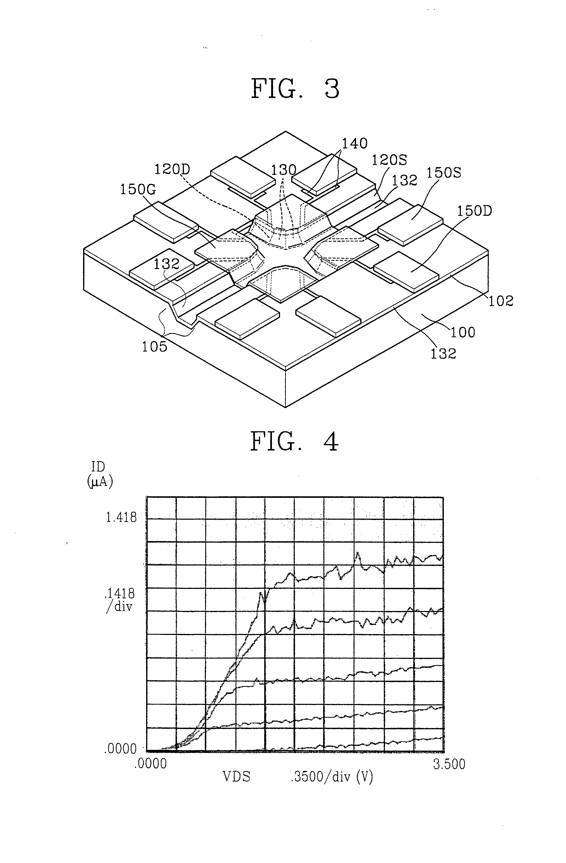
[0107] For quantification of the immobilization of probe DNAs, the chip of FIG. 3 was mounted on the chip mount region 40 of the molecular detection kit 10 of FIG. 1, and a voltage was applied. Synthetic DNA probes (5-thiol-GTTCTTCTCATCATC-3′) having substituted thiol groups at 5′-terminal were loaded into the sample loading unit 20 in different volumes 20 μL, 40 μL, 80 μL, and 160 μL, respectively, and current variations over time were measured.

[0108] The results are shown in FIG. 16. As shown in FIG.16, as the quantity of probe DNAs loaded into the sensor increases, the current dropping level flowing across the drain and source of the sensor proportionally increases. As a result, the current dropping level was 14 μA for 20 μL of the probe DNA (FIG. 16A), 17 μA for 40 μL of the probe DNA (FIG. 16B), and 20 μA for 80 μL of the probe DNA (FIG. 16C). No increase in current dropping level was observed for more than 80 μL of the probe DNA (FIG. 16D).

[0109...

embodiment 3

on of Probe DNA and Target DNA Hybridization

[0110] For quantification of the hybridization of probe DNAs to a target DNA, a voltage was applied to the lab-on-a-chip of FIG. 3, and synthetic DNA probes (5′-thiol-GTTCTTCTCATCATC-3′) having substituted thiol groups at 5′-terminal and a target DNA having a complementary sequence to the synthetic DNA probe were sequentially loaded. Then, current variations over time were measured.

[0111] The chip of FIG. 3 was mounted on the chip mount region 40 of the molecular detection kit 10 of FIG. 1, and current flowing through the chip was measured with the application of a voltage. Next, a phosphate buffer solution was injected into the sample loading unit 20 of the molecular detection kit 10. Current measurement continued as the phosphate buffer solution was injected. Immediately after the buffer injection, the current level increased, as shown by reference A of FIG. 17. Next, the current level stabilized for about 30 minutes. Then probes of 15 ...


PUM

PropertyMeasurementUnit
temperatureaaaaaaaaaa
volumesaaaaaaaaaa

Abstract

A molecular detection chip including a metal oxide silicon-field effect transistor (MOSFET) on sidewalls of a micro-fluid channel and a molecular detection device including the molecular detection chip are provided. A molecular detection method, particularly, qualification methods for the immobilization of molecular probes and the binding of a target sample to the molecular probes, using the molecular detection device, and a nucleic acid mutation assay device and method are also provided. The formation of the MOSFET on the sidewalls of the micro-fluid channel makes easier to highly integrate a molecular detection chip. In addition, immobilization of probes directly on the surface of a gate electrode ensures the molecular detection chip to check for the immobilization of probes and coupling of a target molecule to the probes in situ.

Description

CROSS-REFERENCE TO RELATED APPLICATIONS [0001] This application is a divisional of application Ser. No. 10 / 239,736, filed Sep. 25, 2002, which is a 35 U.S.C. §371 national stage application of International PCT Application No. PCT / KR02 / 00746 filed Apr. 23, 2002, which claims priority from Korean Application No. 2001-21752, filed Apr. 23, 2001, Korean Application No. 2001-29729 filed May 29, 2001 and Korean Application No. 2001-78010 filed Dec. 11, 2001. The disclosure and content of each of these applications are incorporated by reference herein in their entireties.BACKGROUND OF THE INVENTION [0002] 1. Field of the Invention [0003] The present invention relates to a molecular detection chip including a metal oxide semiconductor field effect transistor (MOSFET) formed on sidewalls of a micro-fluid channel, and a molecular detection device employing the molecular detection chip. Also, the present invention relates to a molecular detection method using the molecular detection device, a...

Claims


Application Information

Patent Timeline
Patent Type & Authority Applications(United States)
IPC IPC(8): H01L21/22G01N33/53B01L3/00C12M1/00C12M1/34C12N15/09C12Q1/68G01N27/28G01N27/414G01N27/416G01N27/42G01N33/543G01N37/00
CPCB01J2219/00497G01N27/4145B01J2219/00585B01J2219/00596B01J2219/00653B01J2219/00657B01J2219/00659B01J2219/00677B01J2219/00722B01J2219/00725B01J2219/00729B01J2219/00731B01J2219/00743B01L3/5027B82Y15/00B82Y30/00C12Q1/6837G01N33/54373G01N33/5438B01J2219/00511C12Q2565/607
Inventor LIM, GEUN-BAEPARK, CHIN-SUNGCHO, YOON-KYOUNGKIM, SUN-HEE
Owner SAMSUNG ELECTRONICS CO LTD
Why Eureka
Try Eureka