Method and apparatus for delivery of pulsed laser radiation

a laser radiation and pulsed technology, applied in laser beam welding apparatus, chemistry apparatus and processes, manufacturing tools, etc., can solve problems such as laser pulse damage, damage to the substrate, and reaches the damage threshold, and achieve the effect of high throughput ra

Inactive Publication Date: 2007-09-27
UVTECH SYST
View PDF5 Cites 39 Cited by
  • Summary
  • Abstract
  • Description
  • Claims
  • Application Information

AI Technical Summary

Benefits of technology

[0051] The novel pulse laser scanning method and apparatus of the invention allow the processing of sensitive surfaces without causing damage, at high throughput rates using near-visible and visible pulsed laser radiation from a small solid state laser with a system that may be operated at room temperature and room pressure. This invention enables the development of advanced semiconductor processes such as cleaning of highly sensitive low-k and other thin film surfaces that cannot now be done with conventional related art methods.

Problems solved by technology

If the total deposited energy density on and in the substrate becomes too great, it reaches the damage threshold.
If laser pulses are deposited such that they are too adjacent in time and / or space, such that the time between pulses is less than the thermal diffusion time, there is the potential for damage to the substrate.
Laser pulse damage is caused by energy being deposited, adjacent in time and space, on and into the substrate.
In an attempt to solve this problem, the pulse overlap can be eliminated by spreading pulses out, but this creates a larger problem of incomplete laser coverage of the substrate.
Unfortunately, the pulse separation used to avoid the overlap ‘damage’ zone results in a larger zone of untreated substrate 20.
In a cleaning application, incomplete coverage results in incomplete cleaning, which is unacceptable and may require a second or third pass, greatly increasing the processing time.
In some cases complete cleaning is not possible without a better method of placing the laser pulses.
This results in an overlap zone where pulses are adjacent in both time and space where the heat from the deposited laser energy is not able to completely dissipate before the next pulse deposits its energy in the same location.
The problem is reduced but not eliminated by the use of square or hexagonal beams, since small but unavoidable errors in beam placement inevitably result in skipped or overradiated regions between pulses.
In processing of delicate or sensitive surfaces, including for example the manufacture of semiconductor devices, thin film heads, optical thin film devices, and flat panel display substrates, this overlap zone will cause a number of unwanted effects which are application dependent.
Firstly, in curing of light sensitive films, the overlap zone will result in an unwanted change in chemical properties of the film from heat buildup, causing an unacceptable dimensional change in the image.
Secondly, in the process of oxidation or oxide or other film growth on a substrate, the temporal and spatial adjacency of pulses will create non-uniformity in the growth of the film that is unacceptable.
In the most extreme cases this energy buildup may result in ablation of the oxide layer.
Thirdly, in cleaning applications, the increase in fluence in the overlap zone will result in physical damage to the underlying substrate in the form of cracking, melting, ablation, or other unwanted changes to the substrate.
If the substrate is ablated, the loose particles can contaminate the substrate.
Additionally, if pulses that are sequential in time occur too close together in space, the resulting reactions will compete for the same portions of the surrounding reactive gas atmosphere resulting in a situation in which the reaction is gas starved and will not be able to proceed to completion.
Another cleaning problem with pulsed laser processing occurs when contaminates removed from thin conductive films are placed on top of thicker less conductive or insulating films.
The difference in thermal expansion between two films causes, for example, a thin top layer to stress and crack when exposed to laser radiation.
When exposed to laser radiation the conductive thin film on top of insulating layer will generate stress lines and open cracks causing shorts.
These films are extremely damage-sensitive to all forms of intense radiation and any mechanical stresses, and conventional surface processing methods, such as wet cleaning or ashing, will not reliably produce damage-free results.
Fourthly, in the use of laser processing to cure films, there is often a threshold reaction temperature above which excessive curing or overheating produces undesirable effects.
Laser pulses, placed next to each other as in the related art, will result in very high, non-uniform energy profiles that may overcure the films being processed.
A fifth problem with laser processing is the cost and complexity of the equipment used to deliver laser radiation to surfaces.
Systems of the related art have generally large footprints that consume expensive factory or clean room floor space.
Further, the combined size and complexity of the lasers and optical systems makes the process expensive and prevents the expanded use of laser technology in general for cost reasons.

Method used


Image

  • Method and apparatus for delivery of pulsed laser radiation
  • Method and apparatus for delivery of pulsed laser radiation
  • Method and apparatus for delivery of pulsed laser radiation

Examples


Embodiment Construction

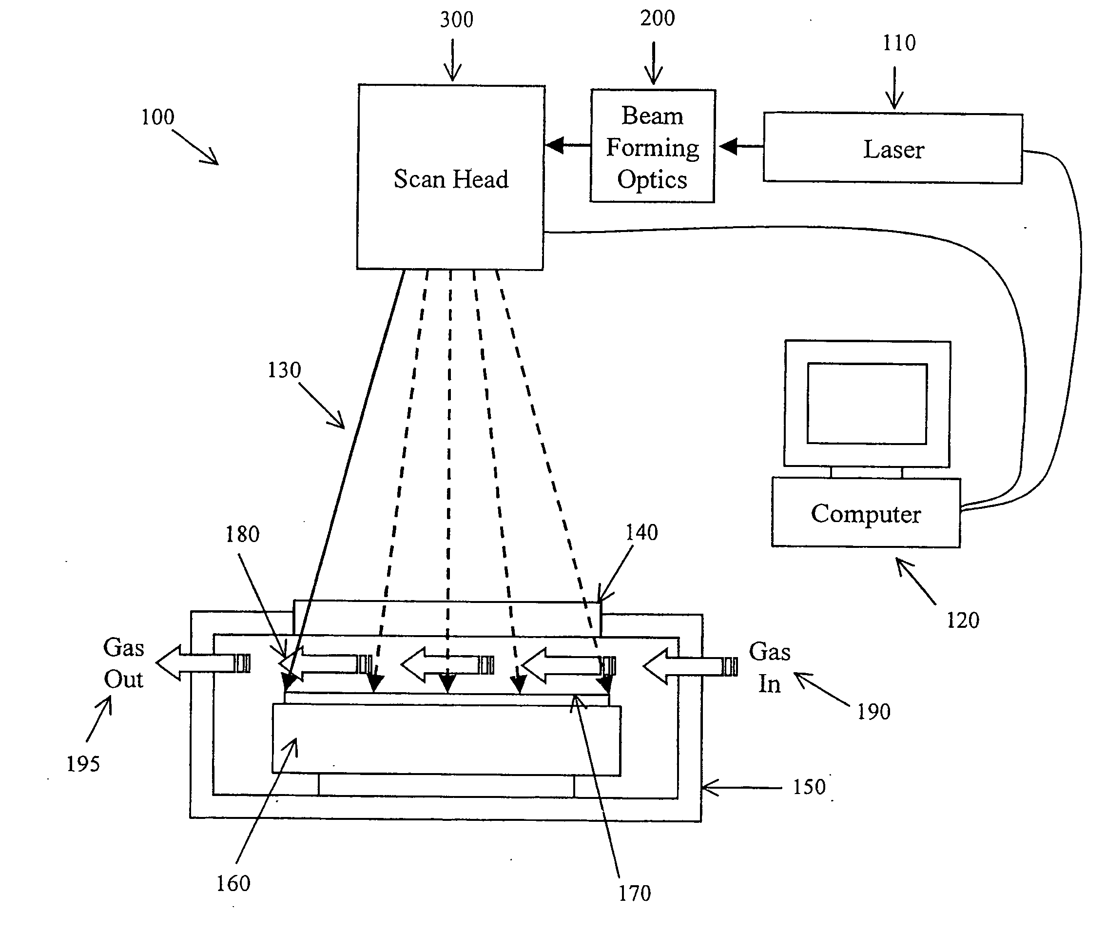
[0070] In the following description of the preferred embodiments of the invention, a method and apparatus for optimally delivering pulsed laser radiation will be detailed.

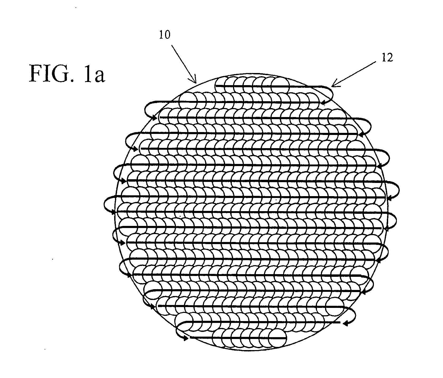
[0071] In FIG. 1a, one of several possible conventional scanning methods is illustrated, a two-dimensional serpentine or boustrophodonic scan. An alternative is to “fly back” at the end of each scanned line so that all lines are scanned in the same direction. Another method is a one-dimensional scan with the substrate stepped in the orthogonal direction.

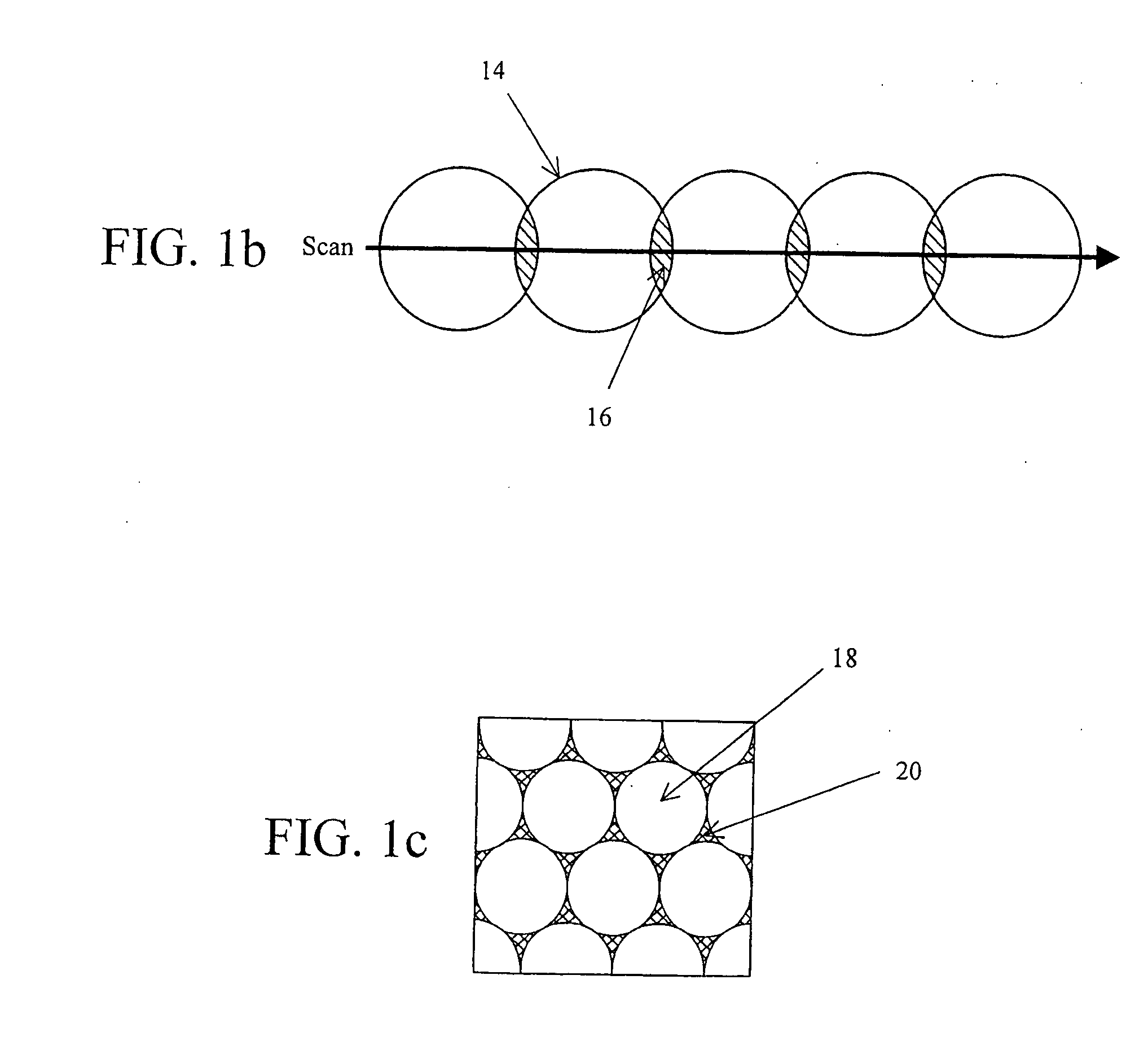
[0072]FIG. 1b illustrates the “double exposure” that results from an attempt, using conventional scanning, to obtain complete coverage. Since the time between pulses is very short (10 to 100 μs) compared to thermal diffusion times that can be on the order of milliseconds, the overlap regions reach higher temperatures and are thereby subject to damage or other unwanted effects.

[0073] If such overlap is avoided by larger pulse-to-pulse spacing, as illustrated in FI...


PUM

PropertyMeasurementUnit
wavelengthaaaaaaaaaa

Abstract

A method and apparatus delivers pulsed laser energy to a damage-sensitive surface. The pulse scanning method and apparatus allow for the deposition of a total dose of laser radiation that could not be attained by any conventional means without damaging the substrate being exposed. Using a solid-state diode pumped YAG laser and an enclosure with a gas ambient, laser pulses are scanned across a substrate according to one of several programmed approaches. Pulses are deposited that are non-adjacent in time, or non-adjacent in space, or both; conventional methods have the pulses adjacent in both time and space. Using the various approaches of the invention, the degree of spatial and temporal adjacency can be precisely controlled to permit significant laser radiation doses without causing any substrate damage. The present invention novel method and apparatus can be carried out by integrating a computer, laser and scan head with a small chamber into which gas can flow to permit a variety of surface reactions on damage-sensitive substrates that could otherwise not be conducted with conventional methods and systems.

Description

RELATED APPLICATION [0001] This application is related to U.S. Provisional Patent Application Ser. No. 60 / 776,211, filed in the U.S. Patent and Trademark Office on Feb. 24, 2006, the entire contents of which are incorporated herein by reference.FIELD OF THE INVENTION [0002] The present invention relates generally to a method and apparatus for the treatment of damage-sensitive surfaces with pulsed laser radiation. The present invention provides a novel method and apparatus for processing substrates with laser light using a number of pulse delivery approaches that permit laser radiation to be evenly deposited so as to prevent damage to the substrate. The invention is directed toward a method and apparatus for producing laser and gas reactions on damage-sensitive surfaces, such as for advanced semiconductor wafer processes and optical thin film surfaces. It finds particular application for damage-free treatment and conditioning of delicate surfaces used in the fabrication of semiconduc...

Claims


Application Information

Patent Timeline
Patent Type & Authority Applications(United States)
IPC IPC(8): H01L21/336
CPCB08B7/0042B23K26/063B23K26/0639B23K26/0643B23K26/0648B23K26/127B23K26/0807B23K26/12B23K26/123H01L21/268B23K26/0665B23K26/0622B23K26/064B23K26/082
Inventor CHAPLICK, VICTORIA M.HARTE, KENNETH J.MILLMAN, RONALD P. JR.ELLIOTT, DAVID J.
Owner UVTECH SYST
Why Eureka
Try Eureka