Organic electroluminescent device

a technology of electroluminescent devices and organic el, which is applied in the manufacture of electrode systems, applications, electric discharge tubes/lamps, etc., can solve the problems of difficult even to bring the internal quantum efficiency close to 1 and the current efficiency of the organic el device is not good, and achieves high current efficiency, good yield, and high reliability.

Active Publication Date: 2007-10-18
SEMICON ENERGY LAB CO LTD
View PDF78 Cites 10 Cited by
  • Summary
  • Abstract
  • Description
  • Claims
  • Application Information

AI Technical Summary

Benefits of technology

[0036] In view of the foregoing, an object of the present invention is to provide an organic EL device that has good yields and high reliability as well as high current efficiency that is realized by introducing the new concept to the conventional organic EL device structure.
[0041] Although the driving voltage increases higher than that of normal devices, the electric current efficiency can be increased by that amount by applying this basic structure of the present invention, similarly to the organic EL device of Non-patent reference 5, which uses the charge generation layer. Moreover, complicated operations in which many layers are laminated can be omitted because a structure may be formed in which conductive particles are dispersed within the EL layer to such an extent that a short circuit does not develop (that is, uniformly). Manufacturing is therefore facilitated as compared with the organic EL device of Non-patent reference 5, which uses a conventional charge generation layer.
[0043] Further, there is also a fear in that the conductive particles 104 will become locally non-uniform in the device shown in FIGS. 1A and 1B, and that short circuit may be caused by insulation damage and the like. It is therefore preferable to use an organic EL device that includes a first electrode 201, a second electrode 202, an EL layer 203, and conductive particles 204 as shown in FIG. 2A. In the structure of the organic EL device, it is preferable that the conductive particles 204 are dispersed in the EL layer 203, and insulating layers 205a and 205b are formed between the first electrode 201 and the EL layer 203, and between the second electrode 202 and the EL layer 203, respectively. It becomes easy to prevent device short circuits by using this type of structure, and at the same time, the development of leak currents can also be prevented by the existence of the insulating layers 205a and 205b. Thus, improved efficiency can be also expected.
[0045] A more preferable structure is designed such that the insulating layers 205a and 205b are made sufficiently thick in the organic EL device of the present invention shown in FIG. 2A so that carriers from the first electrode 201 and the second electrode 202 are not injected. In this case, carriers cannot be injected from the outside, and carrier injection sources (generation sources) can only exist in internal portions of the EL layer 203 (that is, carriers can only be injected from the conductive elements 204). Operation is therefore performed by alternating current drive (FIG. 2B). This procedure is extremely effective in preventing device short circuits, and in particular, can provide devices having superior yield and operational stability.
[0048] Structuring the EL layer by using a single layer structure (that is, a bipolar layer) makes manufacturing easier for the organic EL devices of the present invention, regardless of the structure as in FIGS. 1A and 1B, or FIGS. 2A and 2B, and is therefore preferable. Further, the bipolar layer is particularly preferable when using alternating current drive, in the structure as in FIG. 2B.
[0049] There is a procedure for forming the EL layer by using a bipolar layer in which an organic compound having electron transporting characteristics and an organic compound having hole transporting characteristics are mixed. Further, there is a procedure in which a polymeric compound having bipolar characteristics and having a π-conjugate system or a σ-conjugate system is used. The latter in particular has an advantage in that the EL layer can be formed easily by wet coating concurrently with the conductive particles, and is effective in terms of simplicity of film formation.

Problems solved by technology

However, there is means for applying large amounts of current to the organic material that is essentially insulators.
However, an organic EL device has a problem with respect to the current efficiency.
Therefore, in theory, it is possible to extract at most one photon from the recombination of one hole and one electron, and it is impossible to extract a plurality of photons therefrom.
However, in reality, it is difficult even to bring the internal quantum efficiency close to 1.
However, the range of material choice is unavoidably restricted since a phosphorescent material having high phosphorescent quantum efficiency φp should be used.
That is caused by that the organic compounds that can release phosphorescent light at room temperature are extremely scarce.
(However, two times or more amount of voltage is needed compared to the organic EL device having only one layer).
(However, the structure requires several times or more amount of voltage).
However, when the current efficiency is tried to be improved using a charge generation layer, it is required that a number of EL layers should be laminated and the fabricating process become complicated.
Therefore another defects such as the dispersion of each device, the short-circuit of devices, and the like are apt to be caused.
It has negative effects on increasing throughput for mass production.
The fact causes an increase of the cost.
Therefore an organic EL device including a conventional charge generation layer has high current efficiency, however, causes problems such as yields of device or an increase of the cost.

Method used


Image

  • Organic electroluminescent device
  • Organic electroluminescent device
  • Organic electroluminescent device

Examples


embodiment 1

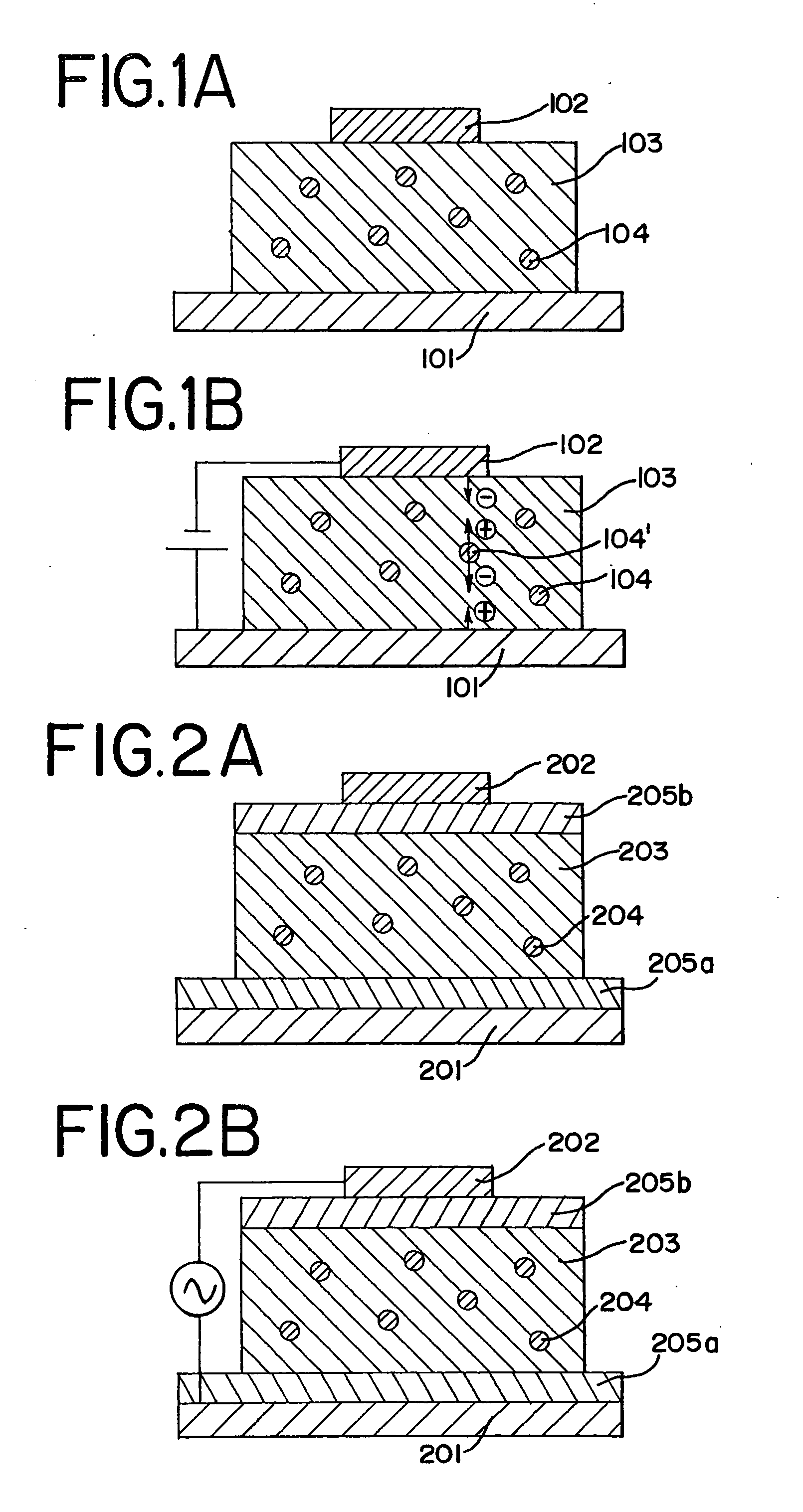
[0080] An organic EL device shown in FIGS. 1A and 1B that is fabricated by wet coating will be specifically described in this embodiment. First, aqueous solution of poly(ethylene dioxythiophene) / polystyrene sulfonic acid (abbrev., PEDOT / PSS) is coated by spin-coating to form a hole injection layer to have a thickness of 50 nm on a glass substrate on which ITO is formed to have a thickness of 100 nm as a first electrode.

[0081] Second, poly(2-methoxy-5-(2-ethyl-hexoxy)-1,4-phenylenevinylene) (abbrev., MEH-PPV) and gold nanoparticles having mean diameter 5 nm stabilized by alkane thiol are mixed in toluene solution. The solution is dispersed enough by using ultrasonic waves and coated 300 nm in thick by spin-coating on the above-mentioned hole injection layer to form an electroluminescent layer.

[0082] Lastly, Al: Li alloy is deposited to have a thickness of 100 nm as a second electrode. Then, an organic EL device can be formed. The organic EL device emits light by direct current driv...

embodiment 2

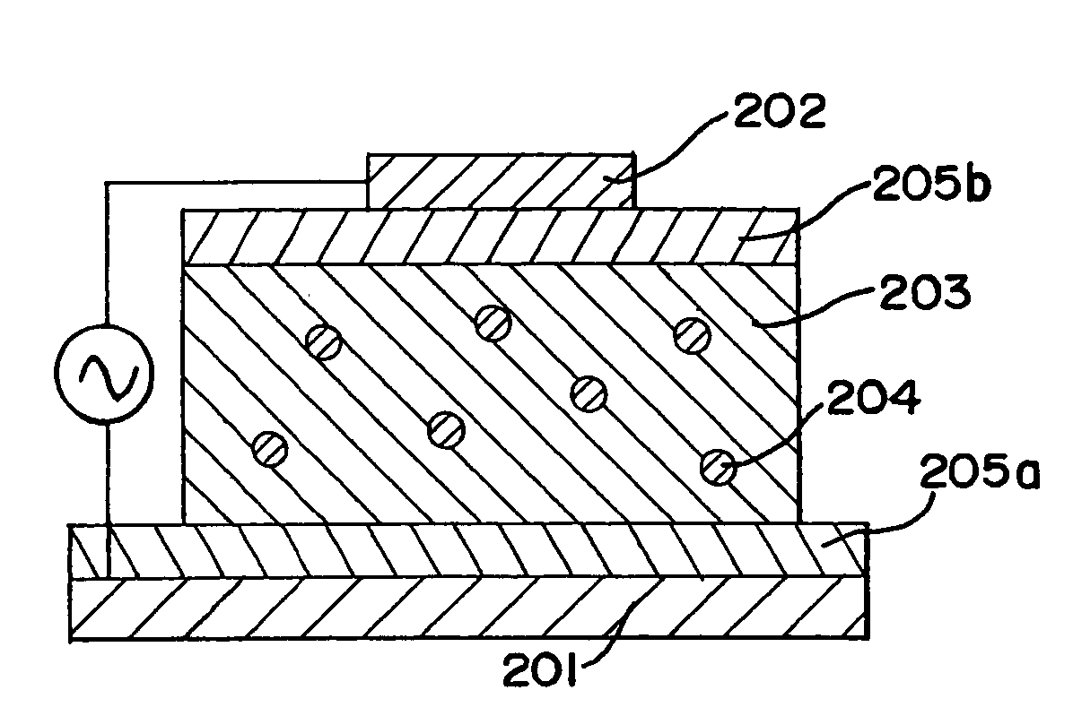
[0083] An organic EL device shown in FIGS. 2A and 2B will be specifically described in this embodiment. First, poly(vinyl phenol) is coated by spin-coating to have a thickness of 200 nm as an insulating layer on the glass substrate on which ITO is formed to have approximately 100 nm in thick as a first electrode. In addition, a material for solvent is isopropanol.

[0084] Then, toluene solution is prepared from 50 wt % polycarbonate as binder, 29 wt % TPD as a hole transporting material, 20 wt % 2,5-bis(1-naphthyl)-1,3,4-oxadiazole (abbrev., BND) as an electron transporting material, 1.0 wt % coumarin 6 as a luminous pigment. The toluene solution is mixed with toluene solution containing gold nanoparticles having mean diameter 5 nm stabilized by alkane thiol. Then, the solution is spin coated on the above-mentioned insulating layer to form an electroluminescent layer to have 300 nm in thick.

[0085] Further, poly(vinyl phenol) is deposited by spin-coating to have a thickness of 200 nm...

embodiment 3

[0086] An organic EL device of the present invention fabricated by bonding and coating with polymer composite films containing luminous pigments and gold nanoparticles without using vapor deposition will be specifically described in this embodiment.

[0087] First, poly(vinyl phenol) is coated by spin-coating to have a thickness of 200 nm as an insulating layer on the plastic substrate (polyester substrate or polyimide substrate) on which ITO is formed 100 nm in thick as a first electrode. In addition, a material for solvent is isopropanol.

[0088] Then, toluene solution is prepared from 50 wt % polycarbonate as binder, 29 wt % TPD as a hole transporting material, 20 wt % 2,5-bis(1-naphthyl)-1,3,4-oxadiazole (abbrev., BND) as an electron transporting material, 1.0 wt % coumarin 6 as a luminous pigment. The toluene solution is mixed with toluene solution containing gold nanoparticles having mean diameter 5 nm stabilized by alkane thiol. Then, the solution is spin coated on the above-men...


PUM


Abstract

An organic EL device that has good yields and high reliability as well as high current efficiency is provided by introducing the new concept to the conventional organic EL device structure. An EL device comprising a first electrode 101, a second electrode 102, an electroluminescent layer 103, conductive particles 104, wherein conductive particles 104 are dispersed in the EL layer 103, is used. Current efficiency will be increased since conductive particles serve as the conventional charge generation layer. In addition, fabricating processes will become simplified and fabricating costs will be reduced because the conductive particles and the EL layer can be formed simultaneously.

Description

BACKGROUND OF THE INVENTION [0001] 1. Field of the Invention [0002] The present invention relates to an organic electroluminescent device having an organic compound layer that generates light upon application of an electric field. [0003] 2. Description of the Related Art [0004] Compared to inorganic compounds, organic compounds have more various material systems and possibilities for synthesizing organic materials to have advanced various functions through appropriate molecular design. Further, things made from the organic compound have characteristics of being flexible, and moreover, having workability by polymerization. In light of these advantages, in recent years, the technique of photonics and electronics employing functional organic materials have been attracted attention. [0005] The technique of photonics utilizing optical properties of organic materials has already played an important role in contemporary industrial technology. For example, photosensitive materials such as a...

Claims


Application Information

Patent Timeline
Patent Type & Authority Applications(United States)
IPC IPC(8): H01J9/00H01L27/32H05B33/14H01L51/50
CPCB82Y20/00B82Y30/00H01L51/5012Y10S428/917H01L51/5278H01L2251/564H01L51/5096H10K50/11H10K50/18H10K50/19H10K71/841H05B33/14
Inventor TSUTSUI, TETSUO
Owner SEMICON ENERGY LAB CO LTD
Why Eureka
Try Eureka