Nonvolatile semiconductor memory devices with charge injection corner

a semiconductor memory and charge injection technology, applied in semiconductor devices, instruments, electrical devices, etc., can solve the problems of reducing the retention life, the scaling for a purpose of speed-up or high integration has been approaching limitation, and the structure is complicated, so as to improve the injection efficiency, speed up the write operation, and reduce the power supply circuit area

Active Publication Date: 2008-11-27
RENESAS ELECTRONICS CORP
View PDF16 Cites 51 Cited by
  • Summary
  • Abstract
  • Description
  • Claims
  • Application Information

AI Technical Summary

Benefits of technology

[0011]A gate electrode 3 is formed on the gate dielectric 2a. The gate electrode 3 is composed of, for example, a polysilicon film, and a silicide layer 4 is formed thereon. A side wall spacer 5 is formed on a side surface of the gate electrode 3. Doped regions 6 and 7 are formed on the main surface of the semiconductor substrate 1 on both sides of the gate electrode 3 in a short direction. Silicide layers 4 are formed on the doped regions 6 and 7. The NROM structure is suitable for scaling or embedding with a logic circuit portion because formation process thereof is simple.
[0012]As a structure suitable for embedding with a logic circuit...

Problems solved by technology

However, it becomes difficult to secure a capacitive coupling ratio required for potential control of a floating gate according to scaling, so that a structure is complicated.
It is necessary to keep a thickness of oxide film surrounding the floating gate to approximately 8 nm or more in order to suppress leakage of retention charges, and scaling for a purpose of speed-up or high integrat...

Method used


Image

  • Nonvolatile semiconductor memory devices with charge injection corner
  • Nonvolatile semiconductor memory devices with charge injection corner
  • Nonvolatile semiconductor memory devices with charge injection corner

Examples


first embodiment

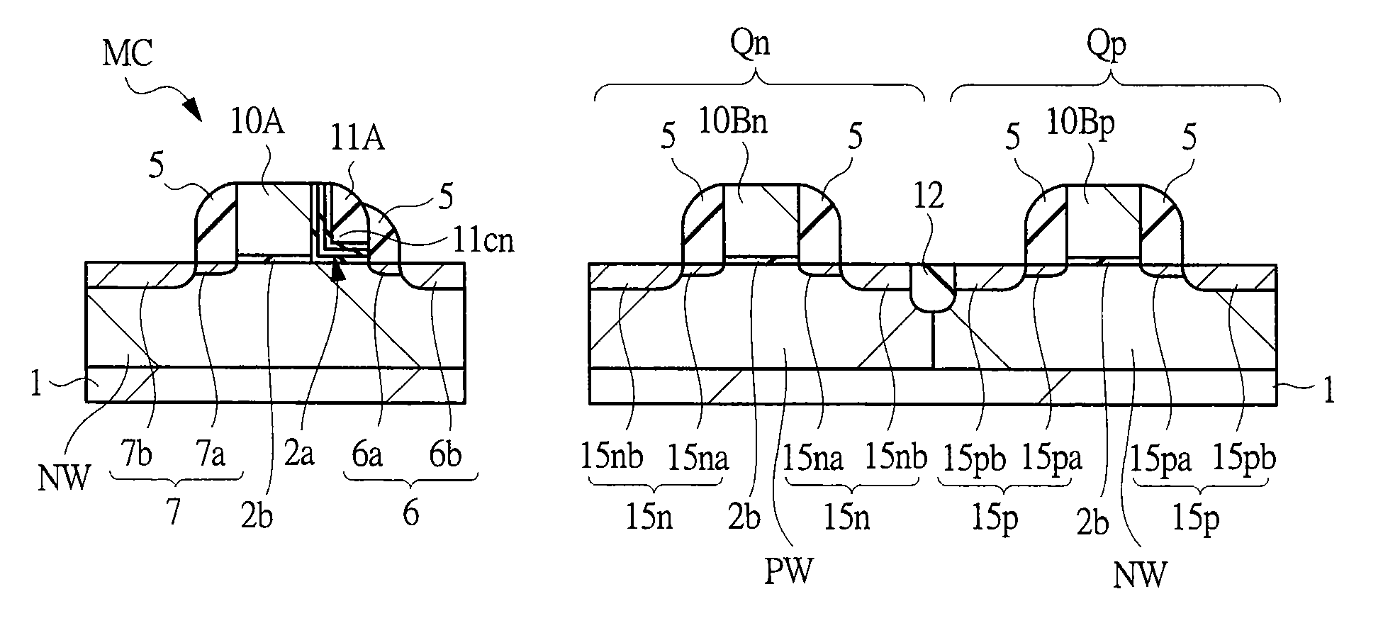
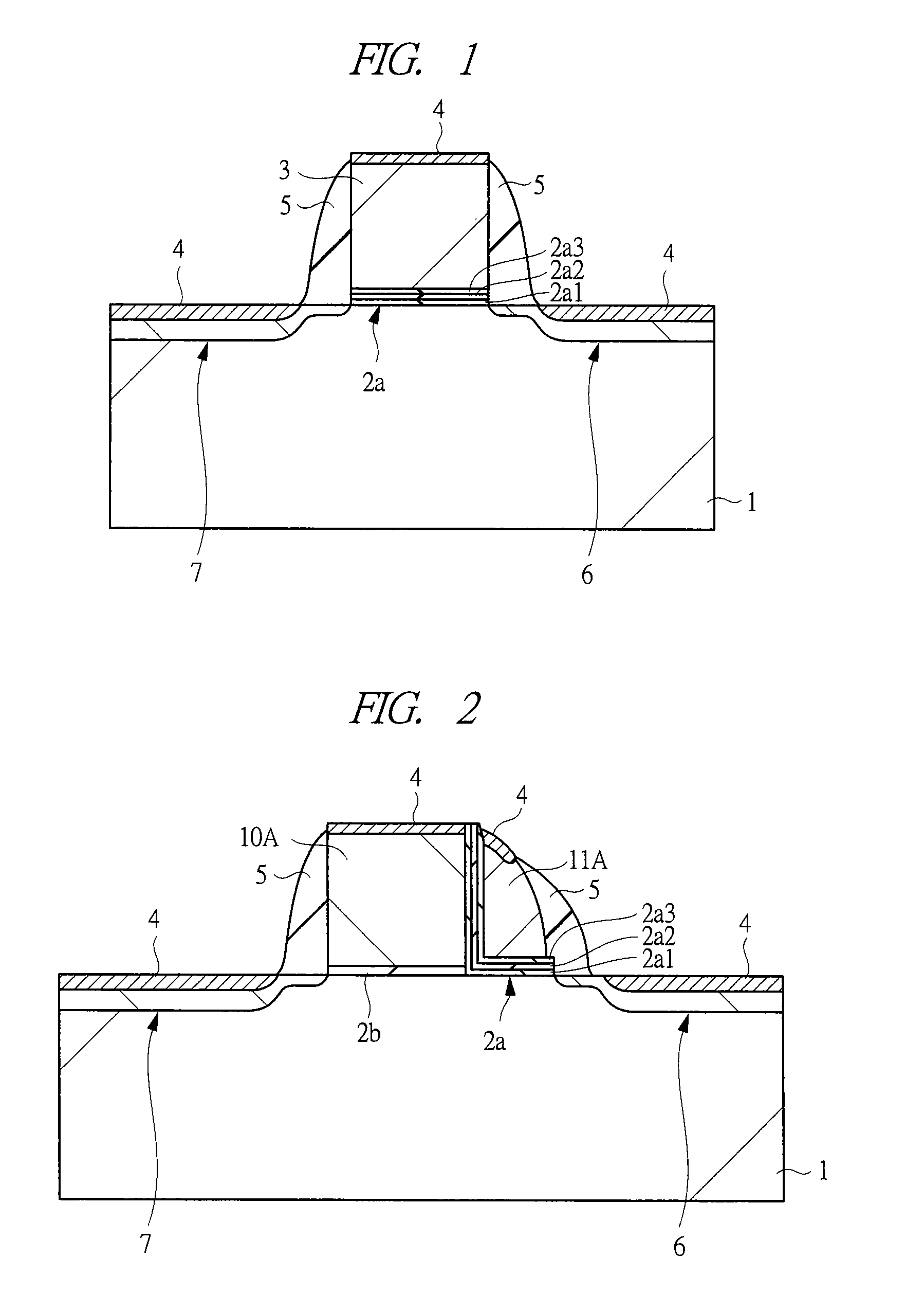
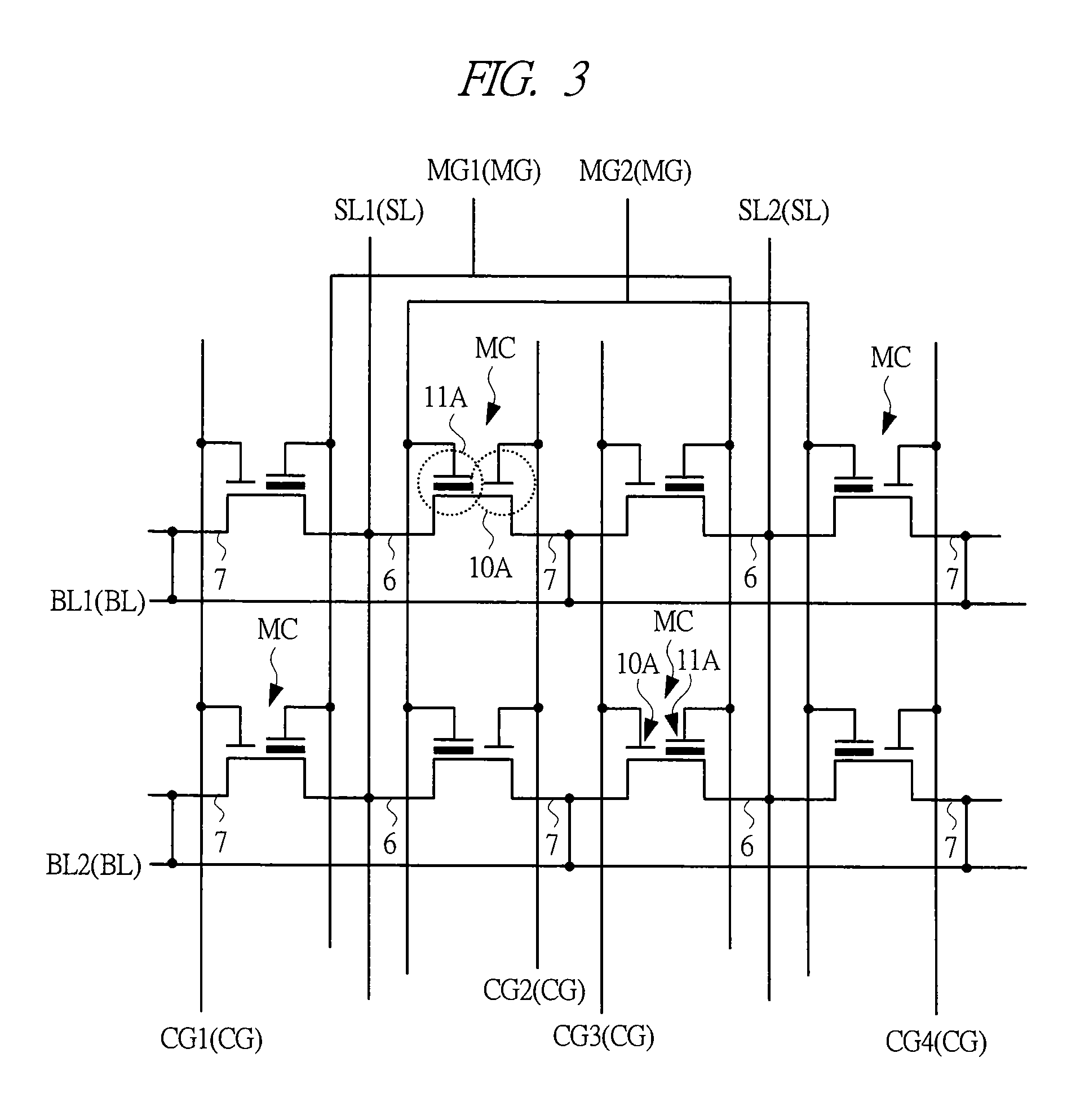
[0095]A semiconductor device according to a first embodiment is a semiconductor device including a logic operation circuit typified by, for example, a microcomputer and a nonvolatile memory circuit provided on one and the same semiconductor substrate. A memory cell (a nonvolatile memory cell) in the nonvolatile memory circuit of the semiconductor device according to the first embodiment is a MONOS memory having a self align split-gate structure. A basic configuration of a memory cell is as explained with reference to FIG. 2 and the like. A memory array configuration is shown in FIG. 3 and a layout of a memory cell MC is shown in FIG. 4. A portion enclosed by a broken line in FIG. 4 corresponds to one memory cell MC. Arrangement of select gate electrodes 10A and memory gate electrodes 11A of memory cells MC adjacent to each other always takes a symmetrical appearance. Incidentally, regarding the above-mentioned terms, here, the term “memory gate electrode” indicates a gate electrode ...

second embodiment

[0119]As a modification of the first embodiment, a semiconductor device according to a second embodiment will be explained with reference to FIG. 29. FIG. 29 is a sectional view of a memory cell MC of the semiconductor device according to the second embodiment. In order to clarify a difference between the first embodiment and the second embodiment, an operation voltage is shown in FIG. 30. Incidentally, FIG. 30 shows a case that a potential of the semiconductor substrate 1 is set to the power source voltage Vcc to read without using any negative voltages and a case that the memory gate electrode 11A is made to be in a non-biased (Vmg=Vsub) retention state.

[0120]A voltage applied to the memory gate electrode 11A at the time of read is set to a voltage of, for example, 1.5 V which is the same power source voltage as the semiconductor substrate 1. A difference from the first embodiment is a memory gate voltage Vmg at the time of read, and by setting this voltage to be equal to that of ...

third embodiment

[0121]A third embodiment is a modification example of the structure of the semiconductor device according to the first embodiment. Part of a manufacturing flow of the semiconductor device according to the third embodiment, which is different from the manufacturing flow of the first embodiment, will be explained with reference to FIGS. 31 and 32.

[0122]First, the same manufacturing process as that of the steps of the first embodiment explained with reference to FIGS. 17 to 19 is performed in this embodiment. At this stage, a select gate electrode 10A is formed on a main face of a semiconductor substrate 1 via a gate dielectric 2b.

[0123]Subsequently, in the third embodiment, dielectric films 20a, 20b, and 20c composed of silicon oxide are formed on a side surface, an upper surface of the select gate electrode 10A, and the main surface of the semiconductor substrate 1 by performing wet oxidization of 6 nm at a temperature of, for example, 800° C., as shown in FIG. 31. In this case, in ...


PUM


Abstract

An erase method where a corner portion on which an electric field concentrates locally is provided on the memory gate electrode, and charges in the memory gate electrode are injected into a charge trap film in a gate dielectric with Fowler-Nordheim tunneling operation is used. Since current consumption at the time of erase can be reduced by the Fowler-Nordheim tunneling, a power supply circuit area of a memory module can be reduced. Since write disturb resistance can be improved, a memory array area can be reduced by adopting a simpler memory array configuration. Owing to both the effects, an area of the memory module can be largely reduced, so that manufacturing cost can be reduced. Further, since charge injection centers of write and erase coincide with each other, so that (program and erase) endurance is improved.

Description

CROSS-REFERENCE TO RELATED APPLICATION[0001]The present application claims priority from Japanese Patent Application No. JP 2007-134085 filed on May 21, 2007, the content of which is hereby incorporated by reference into this application.TECHNICAL FIELD OF THE INVENTION[0002]The present invention relates to a semiconductor device technique, and in particular to an effective technique applied to a semiconductor device having a nonvolatile memory cell including a charge trap film in a gate dielectric among electrically writable and erasable nonvolatile memories such as an EEPROM (Electrically Erasable Programmable Read Only Memory) or a flash memory.BACKGROUND OF THE INVENTION[0003]The electrically writable and erasable nonvolatile memory such as an EEPROM or a flash memory can rewrite a program on board, reduce its development term, and improve its development efficiency. Therefore, the nonvolatile memory can cope with various requirements, such as small-lot multi-product production,...

Claims


Application Information

Patent Timeline
IPC IPC(8): H01L29/792
CPCG11C16/0425G11C16/10H01L27/11526H01L27/11546H01L29/42344H01L29/792H10B41/49H10B41/40H01L21/265
Inventor YASUI, KANISHIMARU, TETSUYAHISAMOTO, DIGHSHIMAMOTO, YASUHIRO
Owner RENESAS ELECTRONICS CORP
Why Eureka
Try Eureka