Method for manufacturing a semiconductor device

a manufacturing method and semiconductor technology, applied in semiconductor devices, semiconductor/solid-state device details, electrical devices, etc., can solve the problems of difficult high-selective etching, and achieve the effect of preventing damage and increasing the surface roughness of the film

Active Publication Date: 2008-12-04
HEFEI RELIANCE MEMORY LTD
View PDF3 Cites 3 Cited by
  • Summary
  • Abstract
  • Description
  • Claims
  • Application Information

AI Technical Summary

Benefits of technology

[0020]For example, in the case where the second metal films mentioned above are each formed of a tungsten film, it is possible to perform a CVD process under the conditions where tungsten hexafluoride (WF6) and hydrogen (H2) are used as a material gas with the temperature being 400° C. Use of the temperature 400° C. can avoid the problem of heat deformation of the organic coating film. In this case, however, fluorine and hydrogen fluoride are produced as reaction by-products. The organic coating film may be etched by these reaction by-products to increase the surface roughness of the film, leading to possible inhibition in the formation of fine contact plugs. In this regard, in the present invention, the organic coating film is covered with a metal-nitride film, such as a titanium nitride film, before forming a tungsten film. Thus, the organic coating film can be prevented from being etched such as by fluorine, with the titanium nitride film serving as a barrier layer. Alternatively, a silicon film may be formed for use as a part of the barrier layer, before forming the metal-nitride film. The silicon film in this case can be formed by a CVD process using disilane (Si2H6) and diborane (B2H6) as a material gas. For generally used phosphor-doped silicon films, monosilane (SiH4) or disilane and phosphine (PH3) are used as a material gas. In this case, a temperature of at least 500° C. or more is required, which may be led to possible heat deformation of the organic coating film. However, in the case of forming a boron-doped silicon film using diborane, the catalytic phenomenon which is characteristic of a diborane material can allow formation of a film at a temperature of 350° C., thus raising no problem of causing heat deformation in the organic coating film.
[0021]According to the present invention, a method for manufacturing a semiconductor device can be provided, which enables formation of fine contact plugs, preventing damages that would be caused by heat deformation or fluorine, even when contact holes are formed in an organic coating film and then the contact plugs are formed using a gas containing fluorine as a material.

Problems solved by technology

This however entails etching of members, such as a silicon nitride film, making it difficult to perform highly selective etching.

Method used


Image

  • Method for manufacturing a semiconductor device
  • Method for manufacturing a semiconductor device
  • Method for manufacturing a semiconductor device

Examples


first exemplary embodiment

[0030]A first exemplary embodiment will be described first, referring to cross-sectional views of FIGS. 4A to 4H illustrating a series of steps. The first exemplary embodiment uses an organic coating film to form contact plugs therein adjacent to word lines.

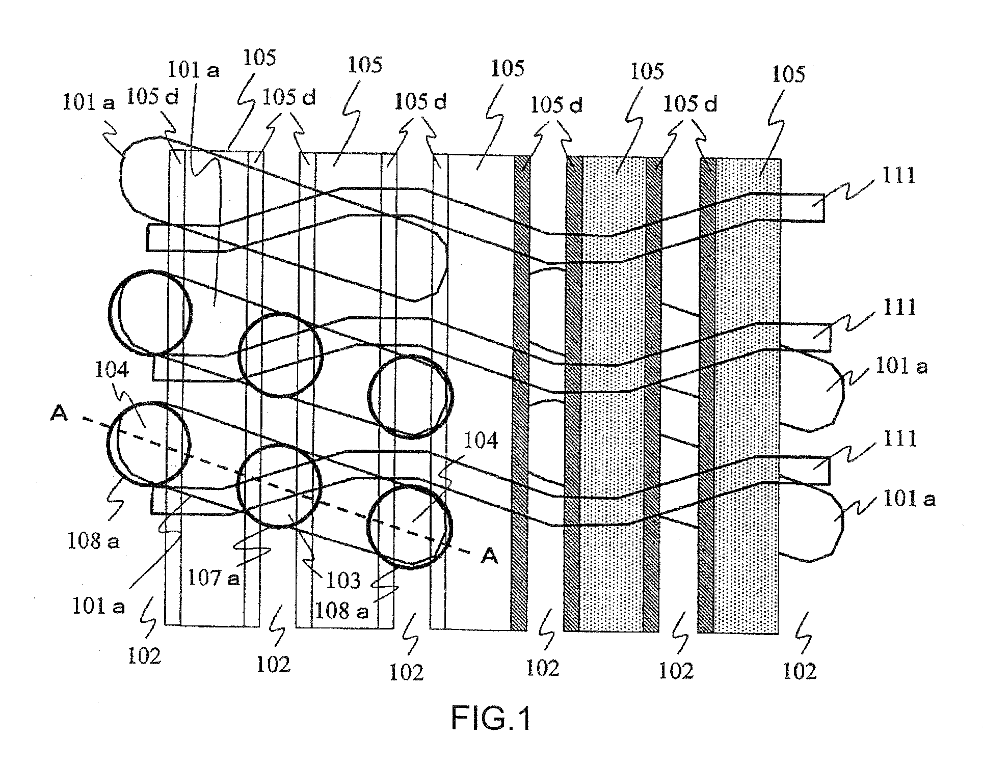
[0031]As shown in FIG. 4A, element isolation regions 102 were formed first, using an STI (Shallow Trench Isolation) process, in the surface of semiconductor substrate 101 made of p-type silicon to form active regions 101a shown in FIG. 1. Then, gate insulating film 105a made up of a silicon oxide film of 6 nm thick was formed on the surface of each active region using a thermal oxidation process. Also, gate electrode 105b of 140 nm thick and protection insulating film 105c made up of a silicon nitride film of 140 nm thick were formed overall. Gate electrode 105b were formed, from bottom up, of a phosphor-doped silicon film and a tungsten silicide film both formed by a CVD process, and a stacked film consisting of a tungsten nitri...

second exemplary embodiment

[0049]As have been described in the BACKGROUND OF THE INVENTION, when forming contact holes in an interlayer insulating film made up of a silicon oxide film, the protection insulating film on the gate electrode and the side walls are each required to be formed of a silicon nitride film in which etching speed is lower than in a silicon oxide film, in order to ensure selectivity of dry etching. Silicon nitride films have inherently been suffering from a problem of increasing parasite capacitance in wiring because of the large dielectric constant. In addition, there is a concern that, when a silicon nitride film is located in the vicinity of a channel of a transistor, function of the silicon nitride film as a charge trap may be a cause of fluctuating threshold voltage of the transistor. In this regard, contact holes in the present invention are formed in an organic coating film which does not require selectivity in etching performed for the silicon oxide film or the silicon nitride fil...

third exemplary embodiment

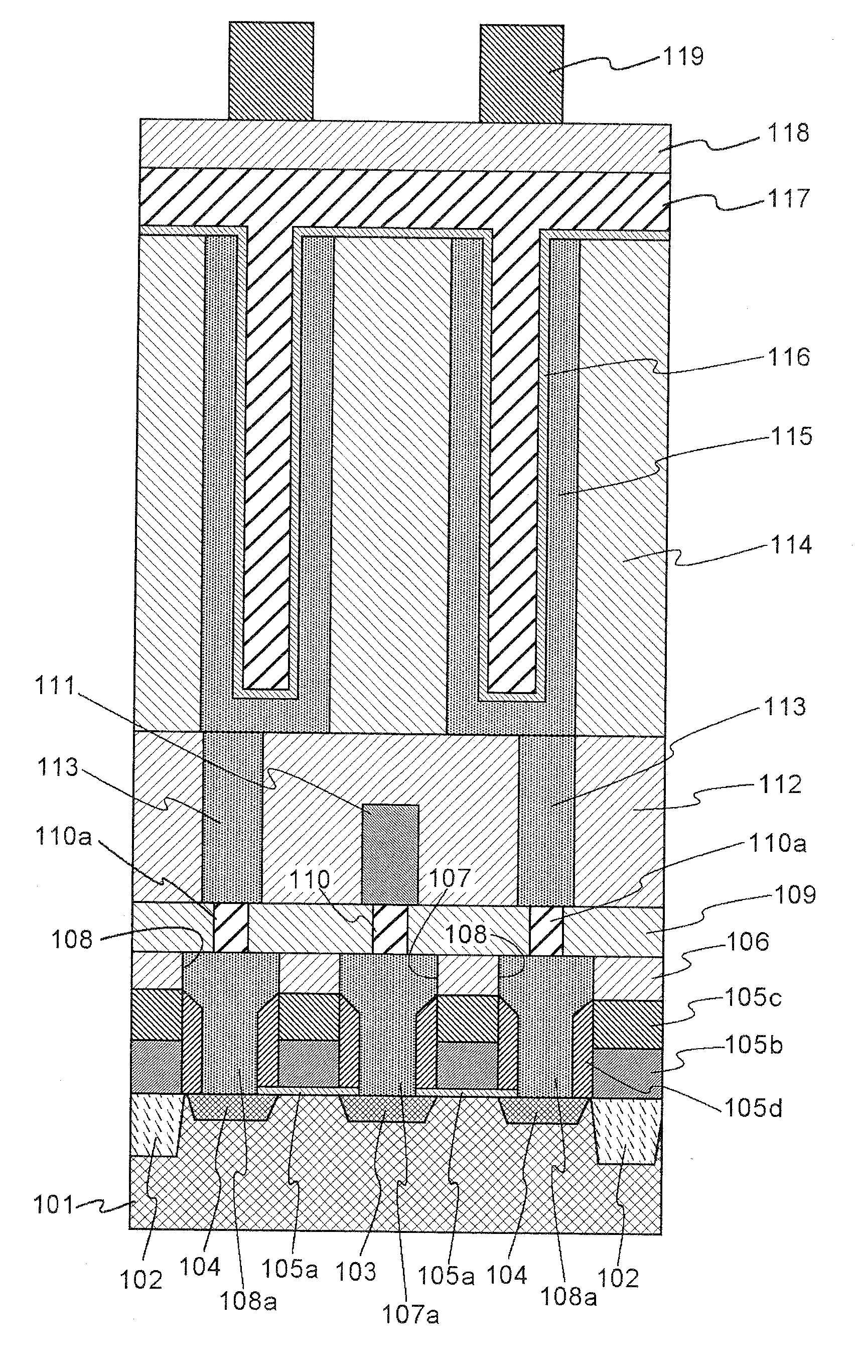
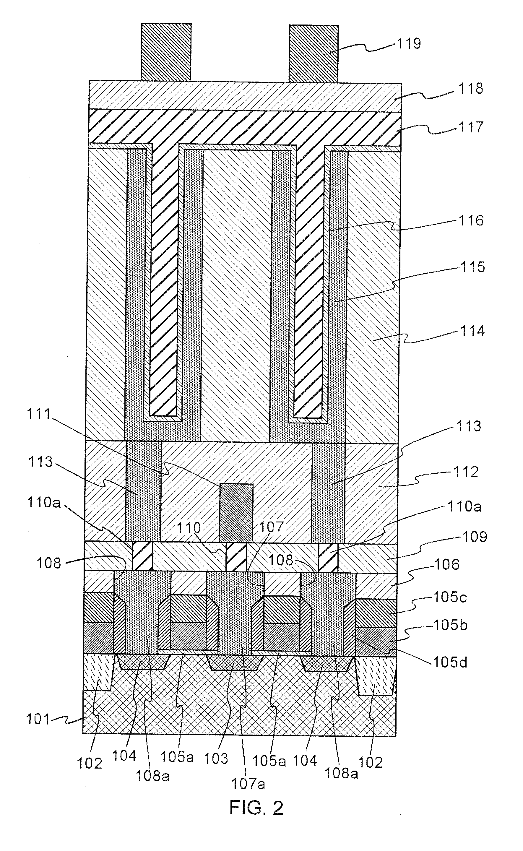
[0056]Referring now to cross-sectional views of FIGS. 4I to 4Q illustrating a series of steps, hereinafter is described a third exemplary embodiment taking an example, in which an organic coating film is used to form the capacitor contact plugs therein adjacent to the bit lines.

[0057]After forming first interlayer insulating film 106 made up of a silicon oxide film of 500 nm thick using an HDP process, as shown in FIG. 4H, the surfaces of contact plugs 107a and 108a were exposed, as shown in FIG. 4I, using a CMP process.

[0058]Then, as shown in FIG. 4J, second interlayer insulating film 109 made up of a silicon oxide film of 150 nm thick was formed, followed by forming second contact plugs 110a including bit-line contact plug 110 in each of predetermined regions in second interlayer insulating film 109. Second contact plugs 110 and 110a were formed by forming contact holes by lithography and dry etching and then by burying the contact holes with a titanium nitride film and tungsten f...


PUM


Abstract

A highly reliable method for forming contact plugs is provided. The method can prevent short circuiting from occurring between self aligned contact plugs and word lines or between self aligned contact plugs and bit lines by applying a material, whose etching speed ratio relative to that of the silicon-based insulating film is 100 or more, to an interlayer film for forming the contact plugs therein. The method comprises forming wiring lines each of which is covered with silicon oxide films at its top surface and lateral sides, forming a sacrificial interlayer film overall, which is made up of an organic coating film without containing silicon, so as to cover the wiring lines, forming contact holes by sequentially etching the sacrificial interlayer film and a lower-layer insulating film, and forming contact plugs. The method further comprises forming columns of the contact plugs by removing the sacrificial interlayer film, forming an interlayer insulating film overall, and partially removing the interlayer insulating film from above the surface thereof to expose the surfaces of the capacitor contact plugs.

Description

[0001]This application is based upon and claims the benefit of priority from Japanese Patent Application No. 2007-048515, filed on Feb. 28, 2007, the disclosure of which is incorporated herein in its entirety by reference.BACKGROUND OF THE INVENTION[0002]1. Field of the Invention[0003]The present invention relates to a method for manufacturing a semiconductor device, and more particularly, to a method for manufacturing a DRAM (Dynamic Random Access Memory) in which a short-circuit margin between a fine contact hole formed by self alignment and an adjacent wiring line has been increased.[0004]2. Description of the Related Art[0005]It is a mainstream trend recently that a DRAM is imparted with a COB (Capacitor Over Bit-line) structure because of the feasibility in ensuring the capacity of the capacitors. In the COB structure, main components of the memory cells include word lines formed on a surface of a semiconductor substrate, bit lines arranged over the word lines through an interl...

Claims


Application Information

Patent Timeline
Patent Type & Authority Applications(United States)
IPC IPC(8): H01L21/4763
CPCH01L21/76897H01L23/485H01L27/10885H01L27/10891H01L2924/0002H01L2924/12044H01L2924/00H10B12/488H10B12/482
Inventor MAEKAWA, ATSUSHI
Owner HEFEI RELIANCE MEMORY LTD
Why Eureka
Try Eureka