Method and apparatus for laser oxidation and reduction

a laser oxidation and reduction technology, applied in the direction of electrical equipment, basic electric elements, semiconductor/solid-state device manufacturing, etc., can solve the problems of large footprint, large equipment floor space, and large particle size of equipment, and achieve high capital cost, high energy use, and significant handling

Inactive Publication Date: 2008-12-04
UVTECH SYST
View PDF42 Cites 27 Cited by
  • Summary
  • Abstract
  • Description
  • Claims
  • Application Information

AI Technical Summary

Benefits of technology

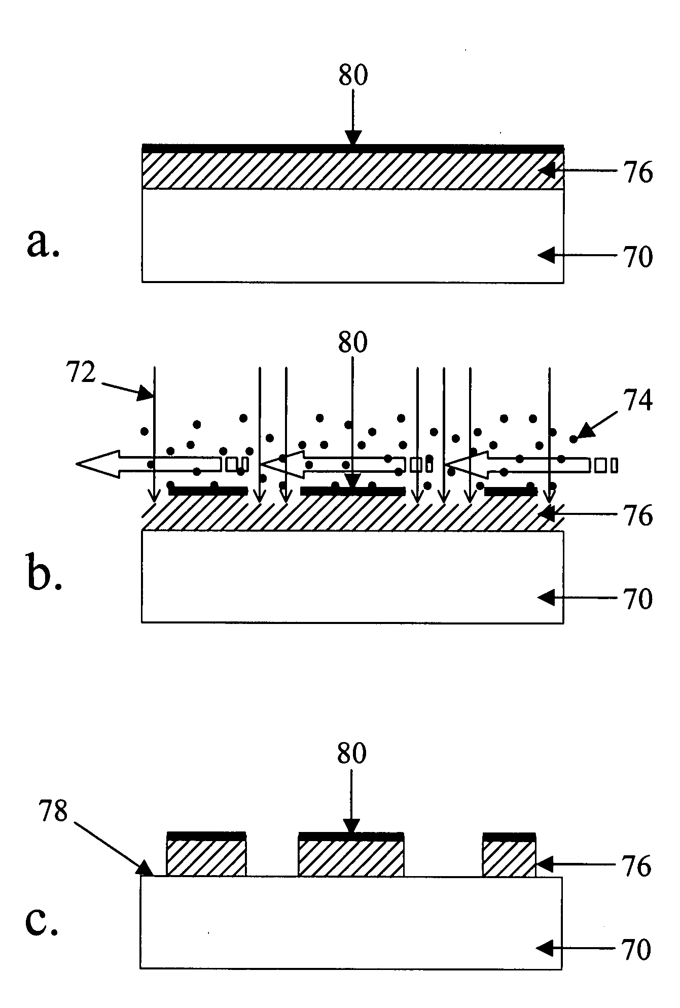
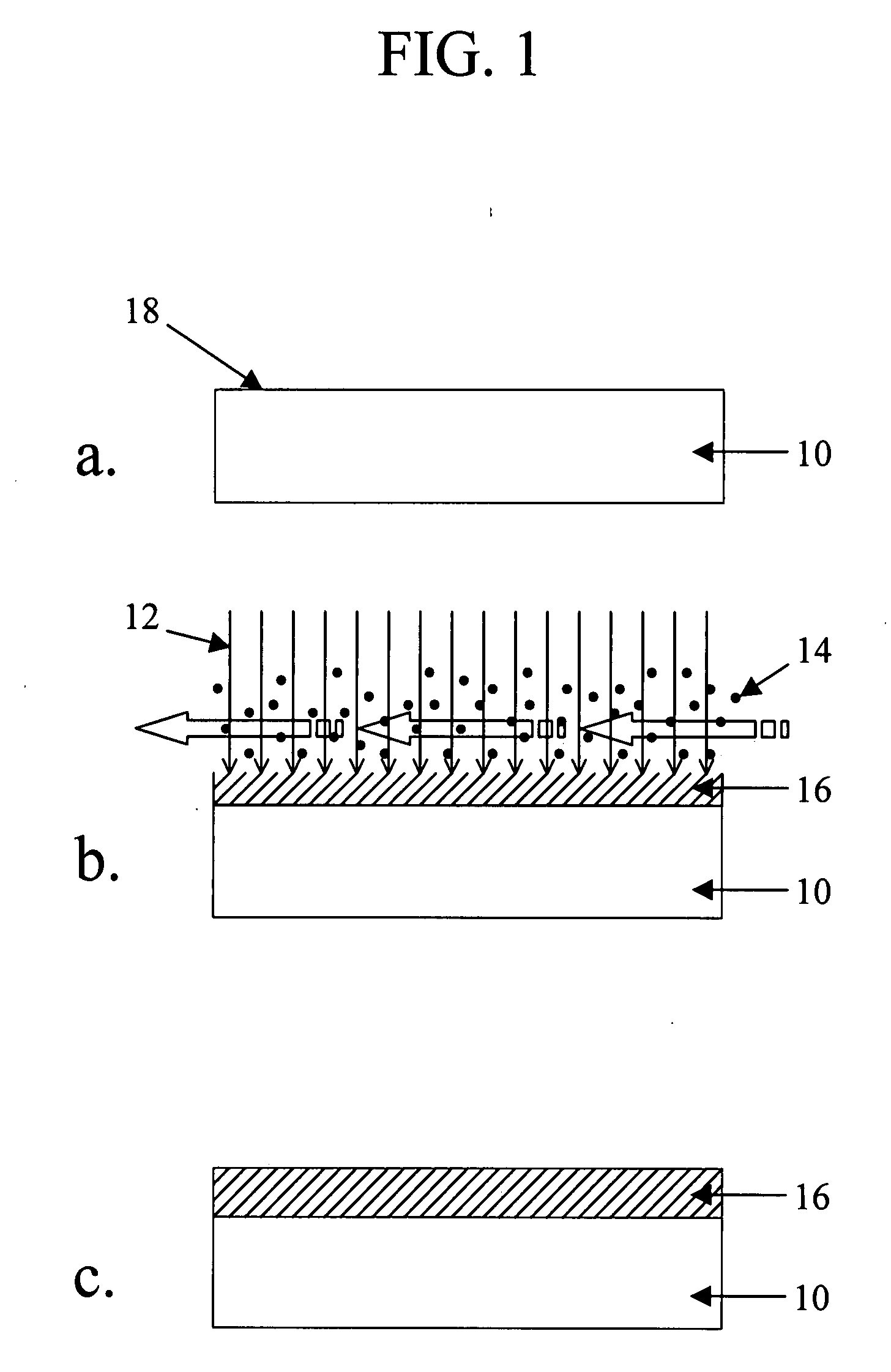
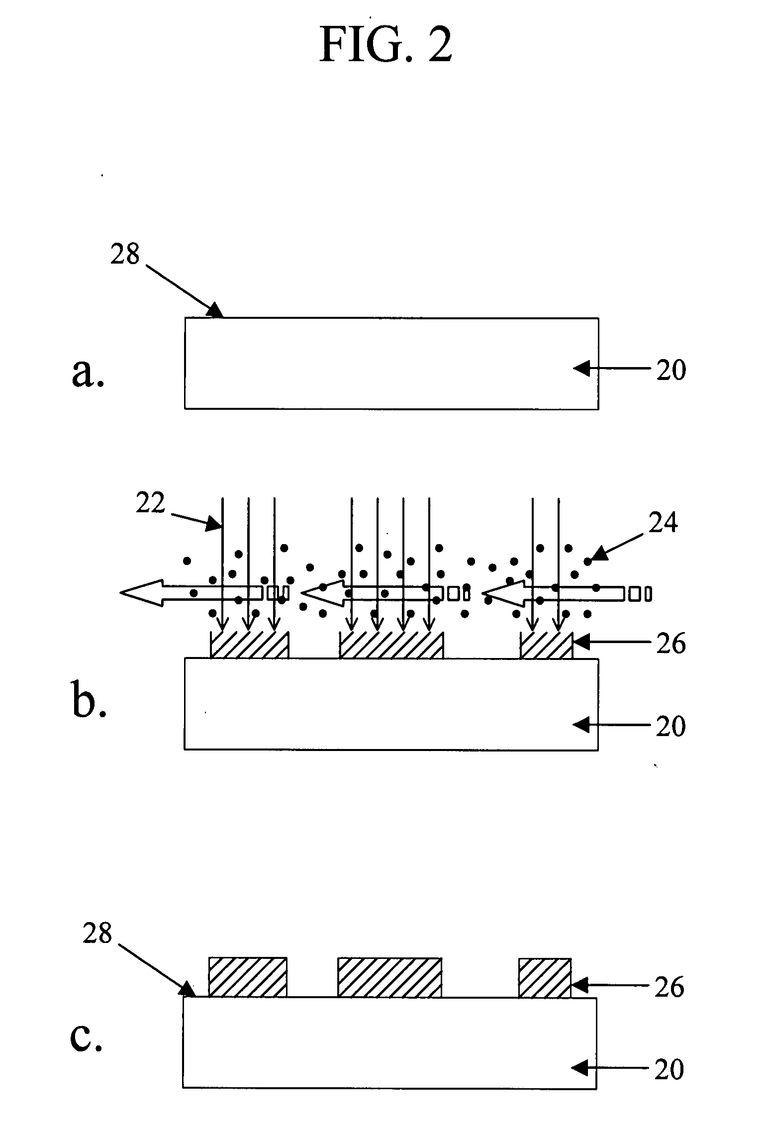
[0023]In one aspect of the invention, a single system is provided that is capable of performing oxidation and reduction-based reactions on a device, thereby alleviating the need for multiple-tools or processes that require significant handling, process time, high energy use, high capital cost, and excessive factory floor space needs. In one illustrative embodiment, a small, robust, simple tool is provided that can perform both oxidation reactions and reduction reactions as used in IC manufacturing. Such reactions may be performed, either alone or in sequence, on a device in the same chamber or other process space, thus avoiding the need to remove the device from the tool when performing both oxidation and reduction processes on the device.
[0024]In another aspect of the invention, a method and apparatus for oxidation and reduction reactions are provided that is environmentally friendly. In one embodiment, oxidation and / or reduction processes may be performed without corrosive and toxic gases or chemicals or requiring extensive waste treatment. ‘Green’ processing is becoming a legislated requirement in many factories.
[0025]In another aspect of the invention, a method and apparatus are provided to perform oxidation and reduction reactions employing low temperatures, e.g., temperatures at or near room temperature. This aspect of the invention may provide for reduced effects on dopant implant depths or other dopant migration, reduced wafer or other device warpage due to heating, and other benefits.

Problems solved by technology

Firstly, as discussed above, high pressure oxidation of silicon used in IC manufacturing typically requires large footprint, complex equipment, thus requiring significant facility floor space.
Further, the size and complexity of this equipment generates particles which become embedded in the oxide film being grown.
In the oxidation of polymers, where oxygen is used to remove organic films and residues from the surfaces of silicon wafers, the same problem of large footprint tools taking up expensive factory floor space exists.
The use of large ashing tools at high temperatures to oxidize resists creates hot particles of polymer that re-deposit onto the silicon surface, and can only be removed with corrosive wet acids and highly corrosive proprietary organic stripping solutions which are highly polluting.
Secondly, oxidation and reduction reactions in IC manufacturing typically require the use of a considerable volume of toxic chemicals and gases that require expensive abatement processes.
The cost and availability of water alone is a major problem.
The cleaning of process chambers requires large volumes of, for example, nitrogen trifluoride, a highly expensive and toxic gas.
In short, related art processes are not environmentally friendly, and are energy intensive.
These high temperatures can cause migration of dopants introduced near the surface of the substrate, resulting in unwanted changes in the electrical properties of the device.
In the high temperature oxidative removal of polymer films, high temperatures in large ashing tools also generate hot sticky particles of resist that redeposit on the wafer and require harsh chemicals to remove.

Method used


Image

  • Method and apparatus for laser oxidation and reduction
  • Method and apparatus for laser oxidation and reduction
  • Method and apparatus for laser oxidation and reduction

Examples


experiment # 1

Experiment #1: Copper Oxidation

[0077]The purpose of the first experiment was to determine whether a 355 nm diode pumped, solid-state laser and an ozone / oxygen gas mixture could oxidize a copper substrate. The chamber pressure used was 30 Torr, with a gas flow of 2 slm and gas composition of 18.5% (by wt.) ozone in oxygen. The vacuum chuck temperature used was 90° C. The pulsed laser beam had a diameter of 417 μm and had been optically transformed into a top-hat beam. The wafer was scanned with a series of 16-interleaved scans, each with a pulse spacing of 400 μm for a final pulse spacing of 100 μm, which equates to a 76.5% overlap.

[0078]The equation to calculate the speed of the beam, which is determined mainly from the laser repetition rate and the spacing between consecutive pulses is as follows: Laser Scan Speed (in mm / s)=Laser Repetition Rate (in kHz)*Single-Scan Pulse Spacing (in μm).

[0079]The laser metrology resulting from this experiment, showing the relevant power readings, ...

experiment # 2

Experiment #2: Copper Oxidation

[0084]The purpose of the second experiment was to determine whether a Gaussian beam profile could produce a more even oxidization of a copper substrate. The chamber pressure used was 30 Torr, with a gas flow of 4 slm and gas composition of 18% (by wt.) ozone in oxygen. The vacuum chuck temperature used was 30° C., which is ambient temperature in the tool. The pulsed laser beam had a Gaussian profile with 1 / e2 diameters ranging from 688 μm to 1664 μm. The first seven sites on the wafer were scanned with a series of 16-interleaved scans, each with a pulse spacing of 400 μm for a final pulse spacing of 100 μm. The final site was scanned with a series of 64-interleaved scans, each with a pulse spacing of 400 μm, for a final pulse spacing of 50 μm.

[0085]The laser metrology resulting from this experiment, showing the relevant power readings, and dose and fluence statistics for each scanned area, along with the scanning parameters for each area, are shown in ...

experiment # 3

Experiment #3: Copper Oxidation

[0088]The purpose of the third experiment was to determine whether a rounded beam profile could produce a more even oxidization of a copper substrate. This profile has a rounded top with a steep drop-off at the edges and can be roughly defined by Equation 1 where F(r) is the intensity of the laser beam profile at a distance, r, from the center and where R is the radius of the beam.

Equation  1:Equation  Defining  a  Rounded  Beam  ProfileF(r)=1-(rR)2

[0089]The chamber pressure used was 100 Torr, with a gas flow of 4 slm and gas composition of 18% (by wt.) ozone in oxygen. The vacuum chuck temperature used was 30° C. The pulsed laser beam had a rounded profile with a diameter of 1400 μm. The wafer was scanned with a series of 16-interleaved scans, each with a pulse spacing of 800 μm for a final pulse spacing of 200 μm, which equates to a 85.7% overlap. Each set of 16-scans is designated as a pass. The areas with multiple passes had the set of 16-scans run...


PUM


Abstract

A method and apparatus using electromagnetic radiation and gas to create oxidation and reduction reactions on a device, such as a semiconductor wafer surface. In one embodiment, a scanned laser and gas may be employed in a number of oxidation and/or reduction reactions in a single system without using multiple pieces of equipment, corrosive chemicals and gases, high temperature and pressure chamber environments, waste treatment processes, and/or extra process steps typically required in existing processes.

Description

FIELD OF THE INVENTION[0001]The present invention relates generally to a method and apparatus for the treatment of surfaces, such as a semiconductor wafer surface, with electromagnetic radiation and gas.BACKGROUND OF THE INVENTION[0002]Oxidation and reduction processes are used, e.g., in semiconductor processing, to both grow films in an additive process, and remove films in a subtractive process. Oxidation reactions are used for at least two primary kinds of processes: cleaning or oxidative combustion of organic films, which is a subtractive process, and oxidative film forming, which is an additive process. Reduction reactions are typically subtractive, and can be used to remove both organic and inorganic films from surfaces. In practice, these processes in the related art have many of the same characteristics and limitations. For example, both oxidation and reduction reaction processes require multiple, separate pieces of complex, expensive equipment that take up considerable fact...

Claims


Application Information

Patent Timeline
Patent Type & Authority Applications(United States)
IPC IPC(8): H01L21/31
CPCH01L21/31116
Inventor ELLIOTT, DAVID J.CHAPLICK, VICTORIA M.
Owner UVTECH SYST
Why Eureka
Try Eureka