

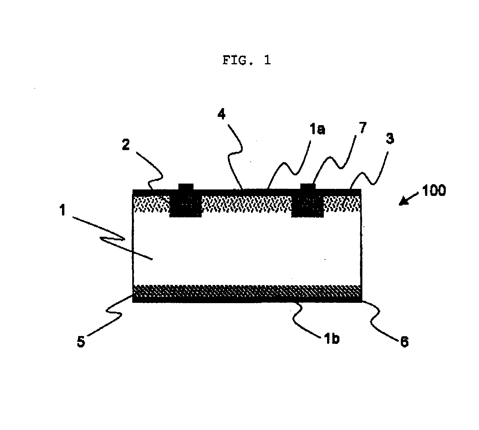
Method for manufacturing solar cell and solar cell, and method for manufacturing semiconductor device
a manufacturing method and technology for solar cells, applied in the direction of final product manufacturing, water-setting substance layered products, chemistry apparatuses and processes, etc., can solve the problems of low fill factor, inability to achieve inability to expect any more significant improvement in conversion efficiency, etc., to achieve easy thermal diffusion of dopant, reduce manufacturing cost, and easy to be coated by a screen printer
- Summary
- Abstract
- Description
- Claims
- Application Information
AI Technical Summary
Benefits of technology
Problems solved by technology
Method used
Image


Examples
example 2
[0146]As a Example 2, the solar cells were fabricated by various fabrication methods of the two-stage emitter of the present invention. Sheet resistances of the high-concentration layer and the low-concentration layer formed at this time were shown in Table 2. Solar cell characteristics thereof were shown in Table 3 along with them.
[0147]In the present example, in order to form the diffusion layers with two concentrations within the same surface by the coating diffusion method, changes in dopant content contained in the coating material, coating film thickness, glass content (silicon compound content), elements, or the like were utilized, as shown in Table 2. In particular, concerning change in coating film thickness, change in viscosity was utilized, or the groove was utilized.
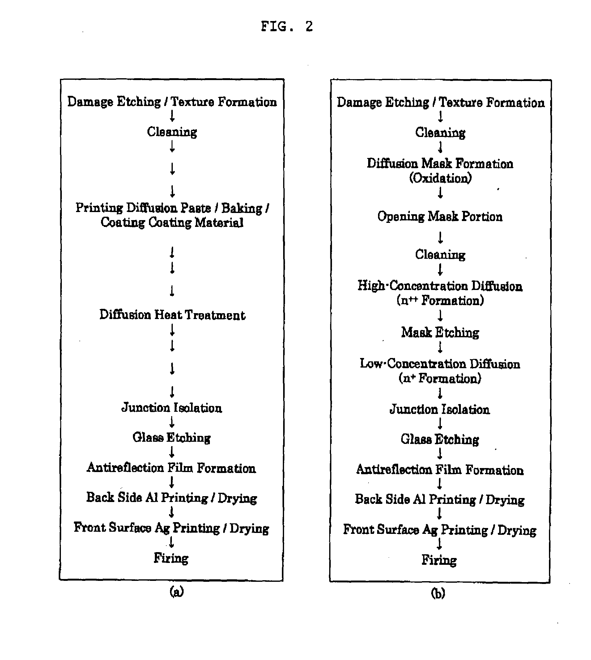
[0148]Hereinafter, the fabrication method for the two-stage emitter will be described briefly. Incidentally, a series of processes from the texture formation and the diffusion to the electrode formation were ...
example 3
[0151]The solar cell was fabricated using the process according to processes A and B shown in FIG. 5. Manufacturing conditions were similar to those of Example 1 other than etch back of the diffusion layer surface, and surface oxidation. In this case, the etch back was performed by dipping the substrate in a mixed-solution of ammonia and a hydrogen peroxide solution after heat treatment to etch the surface by several nanometers. Meanwhile, surface oxidation was performed by making only dry oxygen to flow without decreasing the temperature subsequent to heat treatment to keep the substrate in a heat treatment furnace for 10 minutes. Various characteristics of the solar cell obtained by the present example were shown in Table 4. Incidentally, various characteristics of the solar cell of Example 1 were also shown for comparison. Additionally, spectral sensitivity characteristics (external quantum efficiency) were shown in FIG. 10.
TABLE 4OpenShort circuitConversioncircuitcurrent density...
example 4
[0154]Diffusion heat treatment was performed at 900 degrees C. under an atmosphere a POCl3 vapor-phase diffusion source according to the method shown in FIG. 6. As for other conditions, a diffusion paste and a coating material similar to those of Example 1 were used.
[0155]Averages and standard deviations that indicate the degree of variation of various characteristics of the solar cell fabricated by the aforementioned method were shown in Table 5.
[0156]When the standard deviation within a parenthesis was seen, it turns out that the standard deviation was reduced by the fabrication method for present example, as compared with the case of Example 1. Namely, it can be said that performance variation was improved by the fabrication method for the present example.
TABLE 5OpenShort circuitConversioncircuitcurrent densityefficiencyFillvoltage (V)(mA / cm2)(%)factorExample 40.63436.618.30.790(0.55)(0.11)(0.13)(0.45)EXample 10.63236.518.20.791(0.88)(0.45)(0.31)(0.66)In table, inside of ( ) (par...
PUM
 Abstract
Description
Claims
Application Information