Electronic device and method for producing the same
a technology of electronic devices and electrodes, applied in the field of electronic devices, can solve the problems of high power consumption and unattainable length in view of processing accuracy, and achieve the effect of improving conductivity and superior performance to the devi
- Summary
- Abstract
- Description
- Claims
- Application Information
AI Technical Summary
Benefits of technology
Problems solved by technology
Method used
Image

Examples
first embodiment
Insulated-Gate Field-Effect Transistor
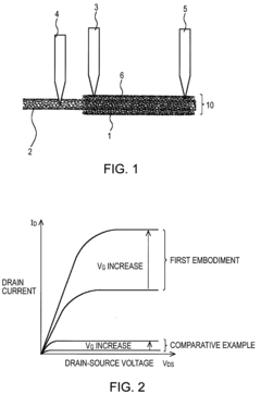
[0104]FIG. 1 is a schematic diagram showing the structure of an insulated-gate field-effect transistor according to a first preferred embodiment of the present invention.
[0105]This field-effect transistor is composed of a multi-walled carbon nanotube 10 having an outer semiconductive carbon nanotube layer 1 and an inner metallic carbon nanotube layer 2 that is partially covered by the semiconductive carbon nanotube layer 1. A metal source electrode 3 and a metal drain electrode 5 are brought into contact with both ends of the semiconductive carbon nanotube layer 1 while a metal gate electrode 4 is brought into contact with the metallic carbon nanotube layer 2.
[0106]To implement transistor operation, a control gate voltage VG is applied to the metallic carbon nanotube layer 2 via the gate electrode 4 while a drain-source voltage VDS is applied to the semiconductive carbon nanotube layer 1 (channel region) between the source electrode 3 and the dr...
second embodiment
Production of Insulated-Gate Field-Effect Transistor
[0112]A process of producing the insulated-gate field-effect transistor according to the first embodiment will now be described.
[0113]
[0114]Multi-walled carbon nanotubes, as a raw material, are prepared by a known method. In thermal CVD (chemical vapor deposition), a hydrocarbon-based source gas is introduced into a reaction tube at a reaction temperature of 600° C. to 1,300° C. to grow multi-walled carbon nanotubes on a catalyst supported by, for example, zeolite placed in the reaction tube.
[0115]The catalyst used is a powder of transition-metal-based fine particles, such as iron, nickel, and cobalt. These particles are supported on the surface of zeolite by, for example, dispersing the zeolite in a mixed solution of iron acetate and cobalt acetate, allowing the zeolite to adsorb the iron acetate and the cobalt acetate, and drying the zeolite.
[0116]The reaction gas used is preferably a hydrocarbon gas such as acetylene (C2H2), whi...
third embodiment
Production of Insulated-Gate Field-Effect Transistor
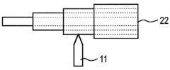
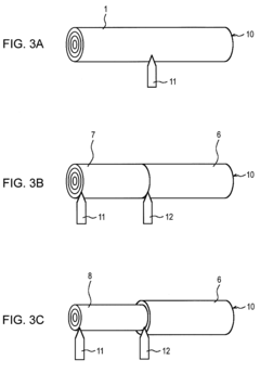
[0137]Another method for producing a multi-walled carbon nanotube having the outer semiconductive carbon nanotube layer 1 and the inner metallic carbon nanotube layer 2 that is partially covered by the inner semiconductive carbon nanotube layer 1 will now be described with reference to FIGS. 5A to 5C.
[0138]First, any multi-walled carbon nanotube 20 is selected.
[0139]The outermost layer of the multi-walled carbon nanotube 20 is then fixed. A first probe 11 is brought into contact with the outermost layer of the multi-walled carbon nanotube 20 in parallel with the axial direction of the multi-walled carbon nanotube 20 in a vacuum chamber. The multi-walled carbon nanotube 20 is left to deposit carbon-containing impurities in the vacuum chamber on the contact portion so that the outermost layer of the multi-walled carbon nanotube 20 is fixed to the first probe 11.
[0140]Next, a second probe 12 is fixed to the inner layers of the multi-w...
PUM
| Property | Measurement | Unit |
|---|---|---|
| current | aaaaa | aaaaa |
| voltage | aaaaa | aaaaa |
| semiconductive | aaaaa | aaaaa |
Abstract
Description
Claims
Application Information