Floating gate having multiple charge storing layers, method of fabricating the floating gate, non-volatile memory device using the same, and fabricating method thereof

a technology of floating gate and charge storage layer, which is applied in the direction of electrical equipment, nanotechnology, semiconductor devices, etc., can solve the problems of easy formation of tunneling oxide films, loss of all charges stored in floating gate, and difficulty in adjusting or controlling the number of charge defects of the inside of the nitride film to capture electrons, etc., to achieve the effect of improving the charge storage capacity of the non-volatil

Active Publication Date: 2009-04-02
KOOKMIN UNIV IND ACAD COOP FOUND
View PDF2 Cites 25 Cited by
  • Summary
  • Abstract
  • Description
  • Claims
  • Application Information

AI Technical Summary

Benefits of technology

[0021]To solve the above problems of the conventional art, it is an object of the present invention to provide a floating gate having multi-layer charge storing layers, a method of fabricating the floating gate, a non-volatile memory device using the same, and a method of fabricating the non-volatile mem...

Problems solved by technology

However, it is hard to adjust or control the number of the charge defects of the inside of the nitride film to capture electrons.
By the way, if a defect or defects occur in the tunneling oxide film which have been formed below the floating gate, all charges stored in the floating gate may be lost.
However, because it is not easy to form the tunneling oxide film very thinly without having defects, charge loss due to defects of the tunneling oxide film may occur more frequently.
By the way, in the case of the non-volatile memory device including nano-crystals, it is not easy to form many nano-crystals in a confined area.
Accordingly, it is hard to secure a sufficient trap site.
Therefore, since there is not a big difference between a threshold vol...

Method used


Image

  • Floating gate having multiple charge storing layers, method of fabricating the floating gate, non-volatile memory device using the same, and fabricating method thereof
  • Floating gate having multiple charge storing layers, method of fabricating the floating gate, non-volatile memory device using the same, and fabricating method thereof
  • Floating gate having multiple charge storing layers, method of fabricating the floating gate, non-volatile memory device using the same, and fabricating method thereof

Examples


embodiment

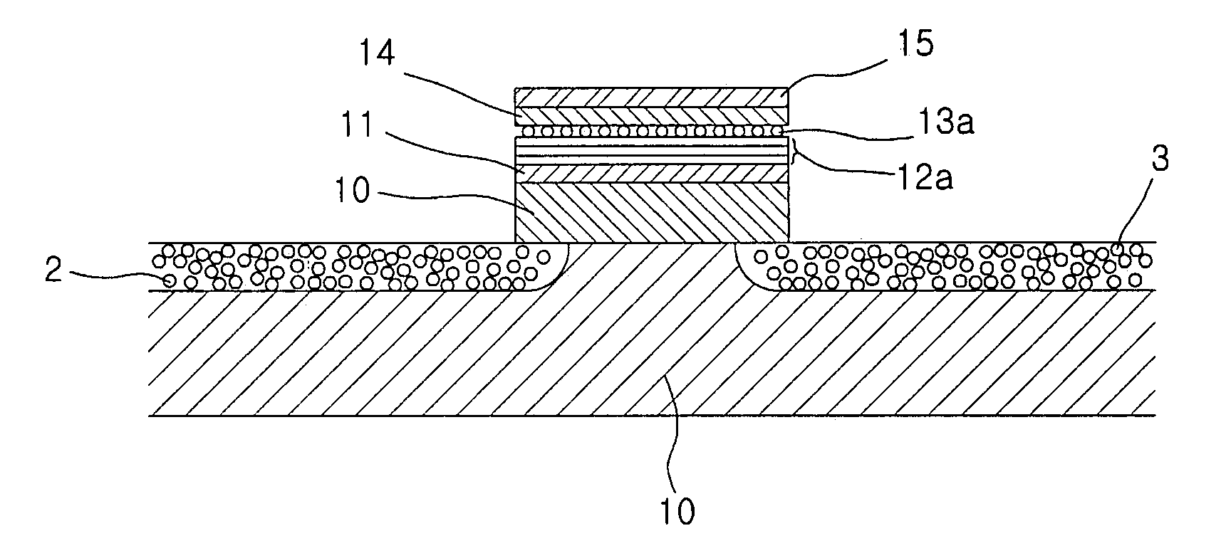
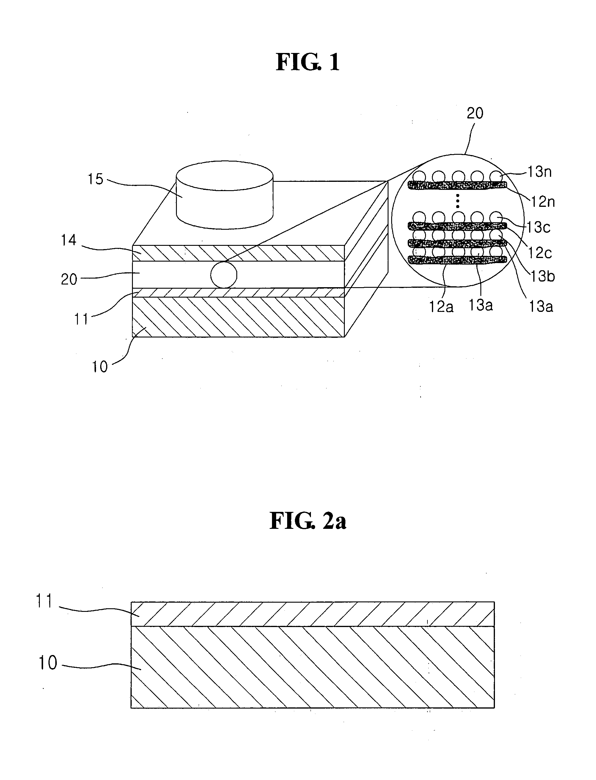
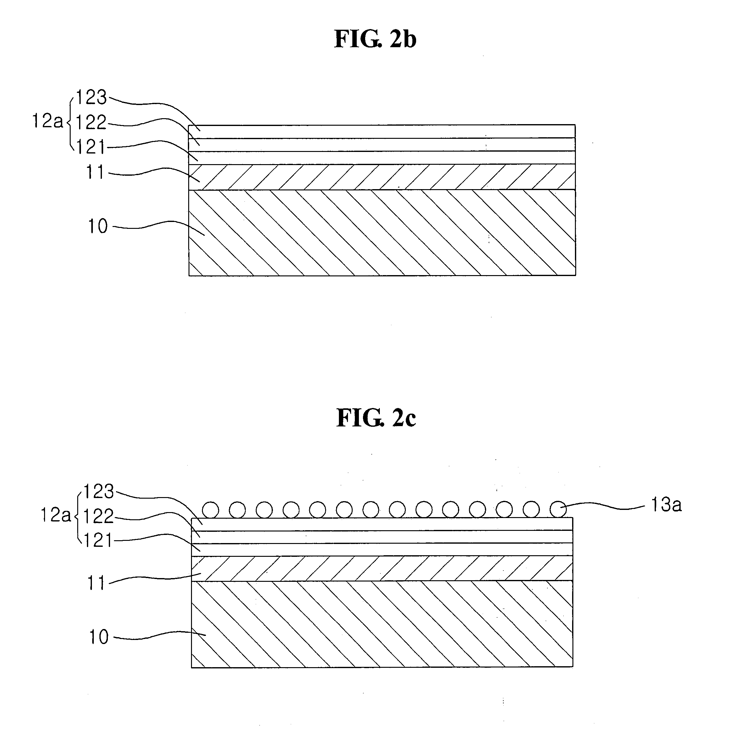
[0131]A. Preparation of a Substrate

[0132]A specimen is manufactured on a p-type silicon substrate (to (100) direction and 1-10 ohm-cm that is made in Siltron company). In the preprocess, the p-type silicon substrate is cleaned using a mixture solution containing sulfonic acid and the hydrogen peroxide at a mixture ratio of 7:3, and then a nature oxide film is removed using a hydrofluoric acid (HF) and washed using ultrapure water.

[0133]B. Formation of a Tunneling Oxide Film

[0134]HfO2 of 0.9-1.9 nm thickness is evaporated as a tunneling oxide film using a RF-magnetron sputtering device. HfO2 evaporation is progressed using a Hf target by a reactive ion sputtering method at an argon and oxygen atmosphere. A base pressure is 10−6 Torr or below, and a process pressure is kept as 20 mTorr.

[0135]C. Formation of Charge Storing Layers

[0136]The charge storing layers (PEs / AuNP)n (here, PEs means polyelectrolyte of PAH / PSS / PAH three layers) are formed on the silicon substrate on which Hf...


PUM


Abstract

Provided is a floating gate having multiple charge storing layers, a non-volatile memory device using the same, and a method of fabricating the floating gate and the non-volatile memory device, in which the multiple charge storing layers using metal nano-crystals of nano size is formed to thereby enhance a charge storage capacity of the memory device. The floating gate includes a polymer electrolytic film which is deposited on a tunneling oxide film, and is formed of at least one stage in which at least one thin film is deposited on each stage, and at least one metal nano-crystal film which is self-assembled on the upper surface of each stage of the polymer electrolytic film and on which a number of metal nano-crystals for trapping charges are deposited. The floating gate is made by self-assembling the metal nano-crystals on the polymer electrolytic film, and thus can be fabricated without undergoing a heat treatment process at high temperature.

Description

BACKGROUND OF THE INVENTION[0001]1. Field of the Invention[0002]The present invention relates to a floating gate having multiple charge storing layers, a method of fabricating the floating gate, a non-volatile memory device using the same, and a method of fabricating the non-volatile memory device, and more particularly, to a floating gate having multiple charge storing layers, a method of fabricating the floating gate, a non-volatile memory device using the same, and a method of fabricating the non-volatile memory device, in which the multiple charge storing layers which use metal nano-crystals of nano size which can easily adjust density and size, is formed to thereby enhance a charge storage capacity of the memory device.[0003]2. Description of the Related Art[0004]A flash memory device which is one of non-volatile memory devices can be largely classified into a floating gate type flash memory device and SONOS (Silicon-Oxide-Nitride-Oxide-Semiconductor) type flash memory device a...

Claims


Application Information

Patent Timeline
IPC IPC(8): H01L29/788H01L21/28
CPCB82Y10/00H01L21/28273H01L29/513H01L29/42332H01L29/42348H01L21/28282H01L29/40114H01L29/40117H01L21/0223
Inventor LEE, JANG-SIKCHO, JINHANLEE, JAEGAB
Owner KOOKMIN UNIV IND ACAD COOP FOUND
Why Eureka
Try Eureka