Method for manufacturing semiconductor device, and method for processing etching-target film
a technology of etching target and semiconductor devices, which is applied in the field of film processing, can solve the problems of increasing the leakage current, reducing the interconnect life, and affecting the influence of the ler formed on the side wall of the line, so as to improve the etching rate of the silicon-containing layer 50, reduce the re-deposition, and improve the efficiency
- Summary
- Abstract
- Description
- Claims
- Application Information
AI Technical Summary
Benefits of technology
Problems solved by technology
Method used
Image
Examples
example 1
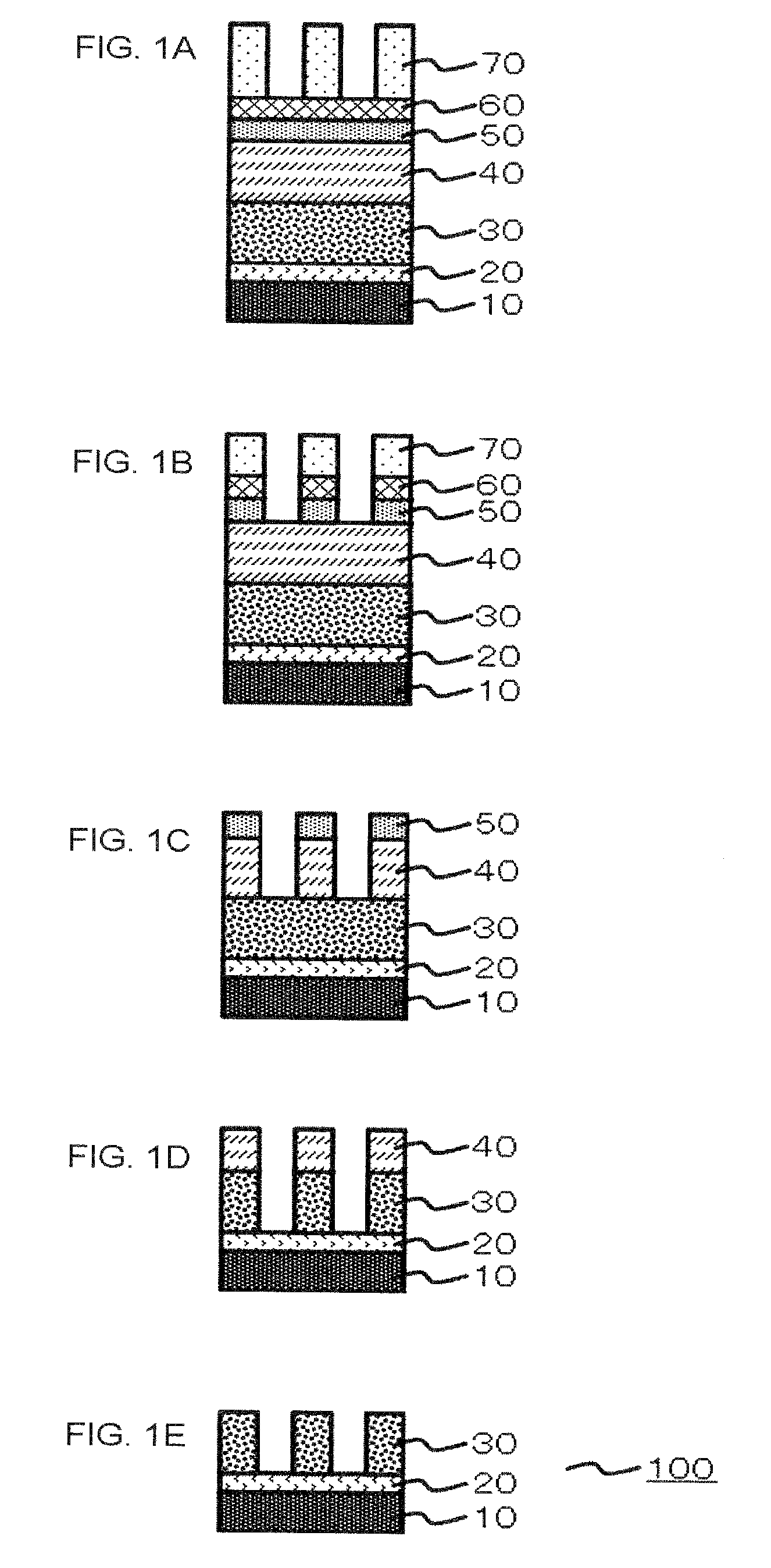
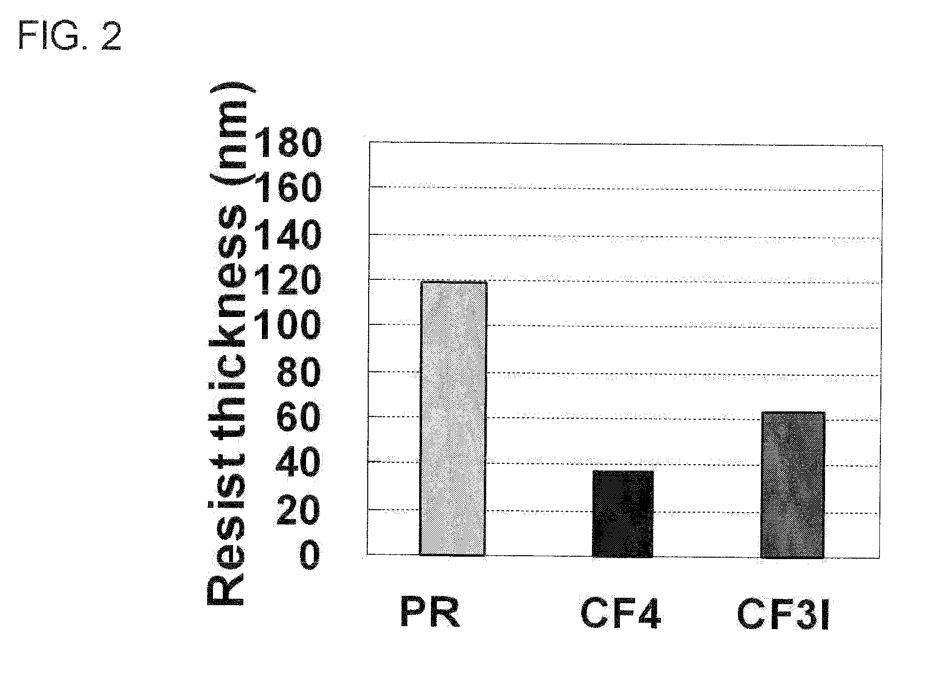
[0075]The first etching operation in the above-described embodiment illustrated in FIG. 1A and FIG. 1B were conducted, and evaluations of the obtained multiple-layered resist films were conducted. More specifically, the etch selectivity of the resist layer 70 over the silicon-containing layer 50 was studied.
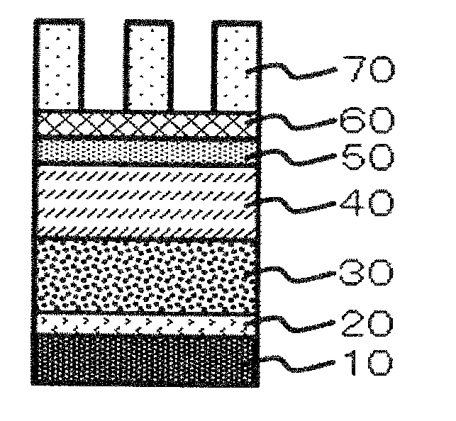
[0076]First of all, an SiO2 film was formed on the silicon substrate, and the following films were sequentially deposited thereon: 30 nm of SiCN serving as the etch stop layer 20; 100 nm of p-SiOC film serving as the interlayer insulating film 30; 60 nm of “dense SiOC” film serving as the cap film; 200 nm of a coated and cured mask composition (TBLM-830: commercially available from Tokyo Ohka Kogyo Co., Ltd.) serving as the organic mask layer 40; 45 nm of a silicon-containing layer 50 (HM series: commercially available from Tokyo Ohka Kogyo Co., Ltd.); 45 nm of a coated and cured composition for an anti-reflection film (ARC 29A: commercially available from Nissan Chemical Industr...
example 2
[0082]The first to third etching operations shown in the above-described embodiment in reference to FIGS. 1A to 1E were conducted, and the obtained interlayer insulating film 30 was evaluated. Specifically, in the present example, p-SiOC trenches with the line interval of 100 nm were formed, and electrical characteristics thereof were evaluated.
[0083]First of all, similarly as in the above-described Example 1, 30 nm of the etch stop layer 20; 100 nm of the interlayer insulating film 30; 60 nm of the cap film; 200 nm of the organic mask layer 40; 45 nm of the silicon-containing layer 50; 45 nm of the ARC 60; and 120 nm of the resist layer 70 were deposited on the SiO2 film formed on the silicon substrate.
[0084]In the present example, an exposure process was conducted by an ArF immersion lithography to form a trench resist pattern with the line interval of 100 nm in the resist layer 70. In such case, a pattern of the interconnect trench 50 nm / space 50 nm (w50 / s50) and a pattern of the...
PUM
| Property | Measurement | Unit |
|---|---|---|
| bias power | aaaaa | aaaaa |
| pressure | aaaaa | aaaaa |
| width | aaaaa | aaaaa |
Abstract
Description
Claims
Application Information


