
Polymeric microfluidic devices from liquid thermoset precursors

Inactive Publication Date: 2009-07-23
HARALDSSON KLAS TOMMY
View PDF5 Cites 5 Cited by
  • Summary
  • Abstract
  • Description
  • Claims
  • Application Information

AI Technical Summary

Benefits of technology

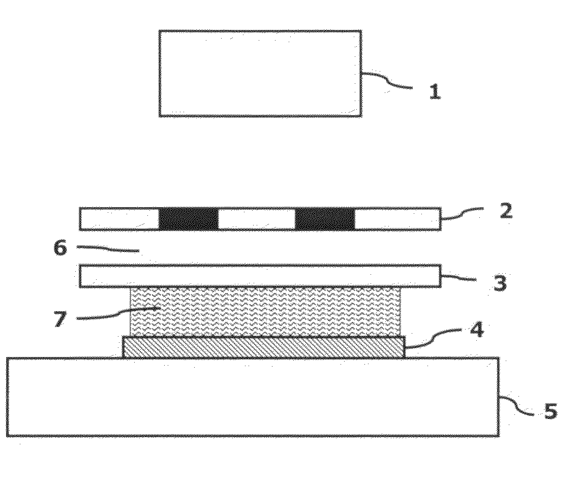
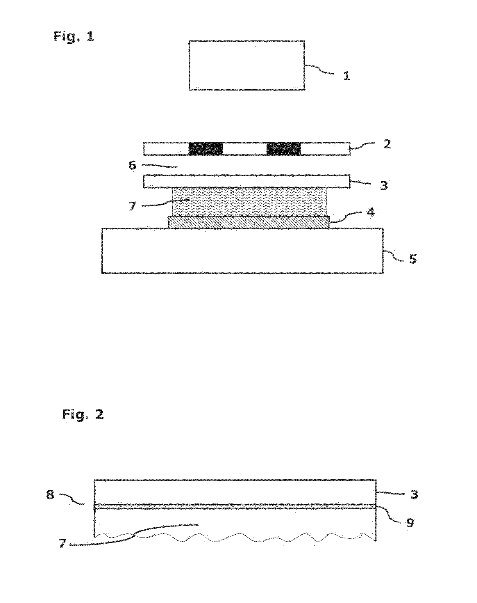
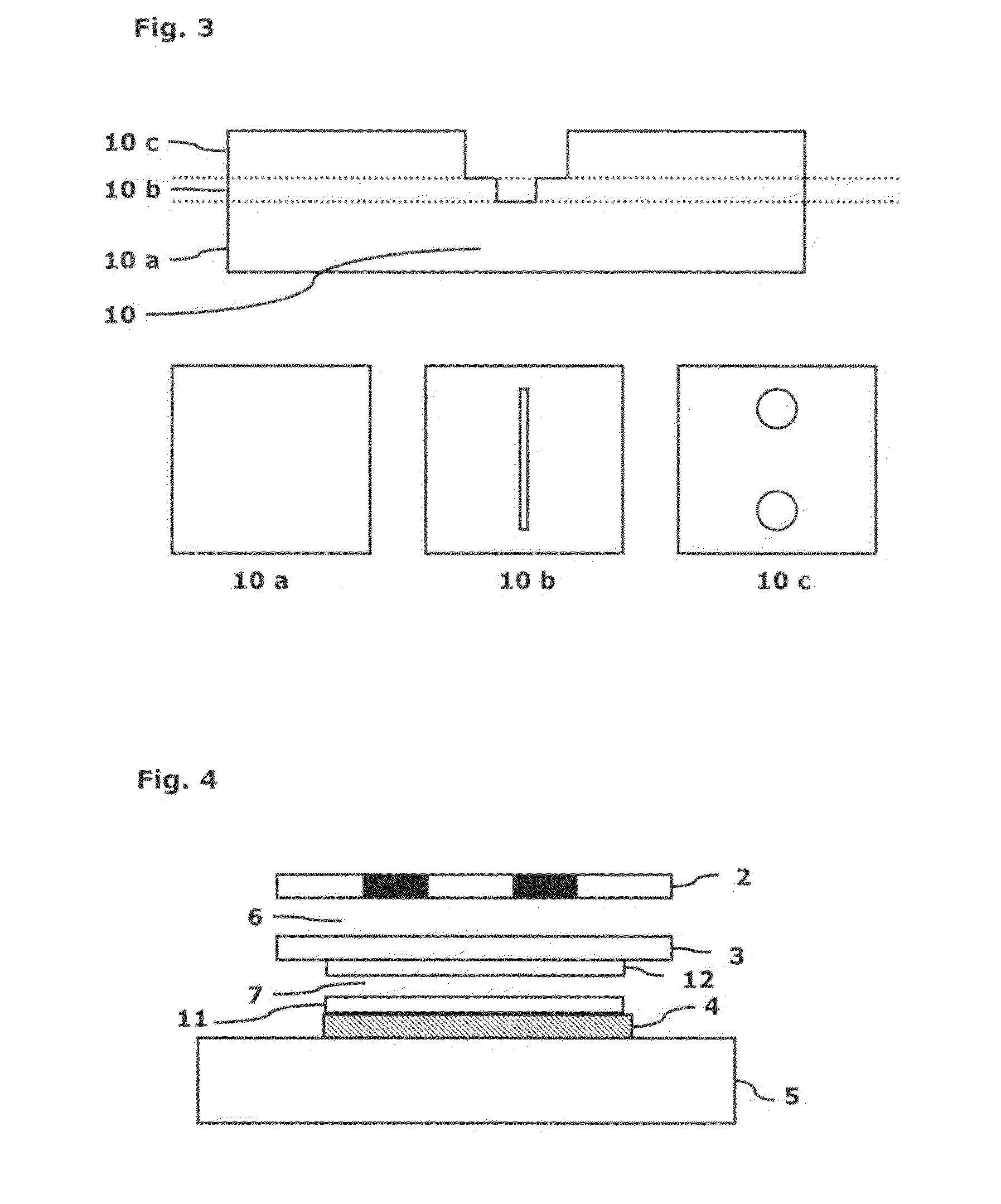
[0032]A primary object of the present invention is to provide a method for the fabrication of a micropatterned polymeric layer with a predefined geometry and predefined materials properties from photosensitive materials through the use of a projected image created by highly collimated UV or visible light passing through a photomask onto a transparent restricting plane underneath which a photosensitive liquid material is immersed between said plane and a substrate. In this manner, a method for inexpensive and rapid mass fabrication of multiple micropatterned layers on a large fabrication area is achieved through the use of a small and inexpensive mask and a projected image that can be moved or magnified to cover fully a fabrication area with multiple individual micropatterned layers. Furthermore, keeping the mask from contact with abrasive or adhesive elements ensures long mask lifetimes, and thus superior fabrication economy. The highly collimated light allows for the fabrication of thick layers which ensures a minimum number of repeating steps, and thus a high production rate. The ability to define micro and macro-patterns via the projected image allows for macroscale facile access points and microscale connected elements.
[0035]To ensure robust enclosure of trenches in order to form channels, sacrificial layers, e.g. wax, may be employed to prevent unwanted polymerization in previously polymerized layers, or a prefabricated lid may be transferred from a transparent rigid plane in a batchwise manner and monolithically incorporated in the device through photoinduced or thermally induced reactions.

Problems solved by technology

However, silicon micromachining is costly, which has led to an increased focus on polymeric microfluidic devices.
These are not yet as advanced as the silicon based devices, but nano-sized patterns and trenches are routinely fabricated on surfaces using nano imprint lithography.
Thus, the problems facing the microfluidics industry are not due to a lack of precision or ability to fabricate very advanced single devices.
Instead, the problems lie in the expense and time consumption for design and fabrication of these devices, where each may take years to perfect.
Furthermore, these devices are not multifunctional platforms as their microelectronic counterparts, e.g. semiconductor processors, but solve a single specific task.
It is almost impossible to economically fabricate specific devices in this manner since each device targets a small niche application.
Also, certain necessary device properties are difficult to routinely fabricate even in singular devices using state of the art methods: 1) connections between the everyday world to chip microfluidic channels and minute reaction chambers via macro to micro interfaces on the device; 2) durable surface chemistries / properties, i.e. surface chemistries that remain unchanged for at least one year and; 3) robust enclosure of trenches in order to form microfluidic channels.
Still, advanced microfluidic applications such as quantitative determination of blood analytes present in low concentration are still not economically or technically feasible.
To date, microinjection molding is only suitable for relatively simple devices in high volume production and is unsuitable for even moderately complex devices due to difficulties in producing undercuts and robust channel enclosure via lid attachment.
Further, materials are limited, and surface modification techniques are generally not reliable for the projected shelf life of microfluidic devices (2 years).
Developments that aim for rational production of microfluidic devices via injection molding are still pursued, but many problems remain unsolved: insufficient materials selection, difficulties in fabricating covered channels and insufficient surface treatment lifetime and quality.
The main problems are fabrication of through-holes since any attempt at producing a through-hole invariably results in a thin blocking polymer layer.
No effective after-treatment process to alleviate the situation has been described.
It is unsuitable for mass fabrication of microfluidic devices due to limited production speed.
The main problems for the fabrication of microfluidic devices with these methods are very limited fabrication speeds due to an excessive number of layers needed for device fabrication and / or poor resolution which prevents accurate fabrication of microfluidic features.
The main problem with this method is inflexibility in material choices for the top and bottom portions of the channel, poor resolution since the curing takes place through a very thick plastic lid, difficulties in surface treatments after the device has been fabricated and unsuitability for massively parallel fabrication due to the use of small prefabricated cassettes.
The main problems with the process described in the articles are the use of collimated light with inadequate collimation (i.e. 2.6 degree half angle beam divergence) and a direct placement of a photomask on top of the glass plate.
The first problem limits the resolution in the polymer to 50-75 micron, according to experimental results, which is an order of magnitude above what is acceptable for microfluidic applications.
The latter problem is problematic for alignment of subsequent layers and limits the illuminated area to the size of the mask since no provision for moving the mask with adequate positional accuracy can be applied.
Further, dust particles or other contaminants on the mask or the glass plate risks introducing air wedges between the glass plate and the mask which in turn may result in Newtonian rings and other optical phenomena that limit patterning accuracy.
The main weakness in this technology is the use of low intensity visible light with nonparallel light beams.
Thus, many layers are needed for the fabrication of full devices which limits the fabrication speed of microfluidic devices to unacceptably low levels.
The main weakness in the process is the contact between the liquid and the photomask.
This presents many problems with mask detachment, mask wear and mask expense when the fabrication area is increased.
The main weakness in this technology is the use of spacers, which are difficult to place with sufficient accuracy to ensure non-tapering layers.
Furthermore, layer thicknesses other than available spacer thicknesses cannot be produced, which severely limits production of multilayer microfluidic devices.
Also, liquid photoresist tends to wick between these spacers and the substrate or surface, resulting in larger than intended resist thickness.
The technologies presented above are almost exclusively incompatible which prevents simple process combinations to achieve mass fabrication of microfluidic devices.
While many of these processes may be suitable for the particular purpose which they address, they are not as suitable for cost beneficial fabrication of polymeric microfluidic devices with good fluidic control, suppressed analyte adsorption, facile access points and adequate handling properties.

Method used


Image

  • Polymeric microfluidic devices from liquid thermoset precursors
  • Polymeric microfluidic devices from liquid thermoset precursors
  • Polymeric microfluidic devices from liquid thermoset precursors

Examples


example 1

[0086]A typical liquid polymer precursor is composed of 1% w / w hydroxycyclohexyl phenyl ketone (Irgacure 184, CIBA, Tarrytown, N.Y.) and 0.5% w / w is an arylsulfonium salt (UVI 6976, Dow, Midland, Mich.) as the photoinitiators, in a mixture of 30% (wt / wt) triethyleneglycol diacrylate (Sartomer, Exton, Pa.), 30% hexavinyl aromatic urethane acrylate (EBECRYL 220, Sartomer) and 40% 3,4-Epoxycyclohexylmethyl-3,4-Epoxycyclohexane Carboxylate (UVR 6110, Dow, Midland, Mich.).

[0087]Typically, to fabricate a single micro and macro patterned polymeric device layer, a glass substrate is placed on the substrate platform of a fabrication machine and held in position with an underpressure distributed in channels machined on the surface of the substrate platform. A photomask is placed in a frame placed above the fabrication assembly and a transparent glass plate (Borofloat, Schott Scientific, Germany) is placed in a frame positioned between the photomask and the substrate. This glass plate is held ...

example 2

[0089]Multilayer devices are fabricated in the same manner as above, with a first layer following the process of Example 1. Layer two utilizes the first layer as a substrate and alignment between features on the first layer and the photomask used for the second layer is ensured using optical or other means and microscrews to move the mask and the fabrication area relative to one another.

example 3

[0090]Multilayer devices with undercuts are fabricated in the same manner as Example 2 until the point where the undercut is reached. The layer that forms the top portion of the undercut is fabricated separately using the transparent plate as the substrate. Turning the transparent plate upside down and securing it in the fabrication machine affords a sandwich like structure where the top is positioned on the contact side of the transparent plate and the bottom portion of the device is positioned on the substrate. A thin layer of liquid polymer precursor consisting solely of TEGDA is applied between the two polymeric portions, a light pressure, where the compressive force is recorded via a sensor, is applied to ensure proper contact between the plates, and the assembly is illuminated for 5-30 seconds to ensure that active species on both polymeric portions polymerize the TEGDA where the portions are in contact / very close proximity. The device is finished similarly to Example 1.


PUM

PropertyMeasurementUnit
Thicknessaaaaaaaaaa
Transparencyaaaaaaaaaa
Reactivityaaaaaaaaaa

Abstract

A method and apparatus for the fabrication of polymeric microfluidic devices through sequential photolithographic polymerization of micropatterned polymeric layers.

Description

CROSS REFERENCE TO RELATED APPLICATIONS[0001]This application claims priority from U.S. provisional application Ser. No. 61 / 002,467 filed Nov. 9, 2007, which is incorporated herein by reference.BACKGROUND OF THE INVENTION[0002]1. Field of the Invention[0003]The present invention relates generally to the fabrication of microfluidic devices and in particular, the fabrication of microfluidic devices via a photolithographic technique that utilizes highly collimated UV or visible light in combination with a binary photomask defined projected image to create micropatterned devices from liquid polymer precursors.[0004]2. Description of the Prior Art[0005]Microfluidic devices are finely detailed constructs designed to deliver precise amounts of fluid to predetermined on-device locations. Typically, microfluidic devices contain minute channels with precise geometries, microreservoirs for chemical reactions and detection windows to allow for external probing of the nature and extent of bioche...

Claims


Application Information

Patent Timeline
IPC IPC(8): G03F7/20G03B27/54
CPCB29C67/0066B29C64/135
Inventor HARALDSSON, KLAS TOMMY
Owner HARALDSSON KLAS TOMMY
Learn More