

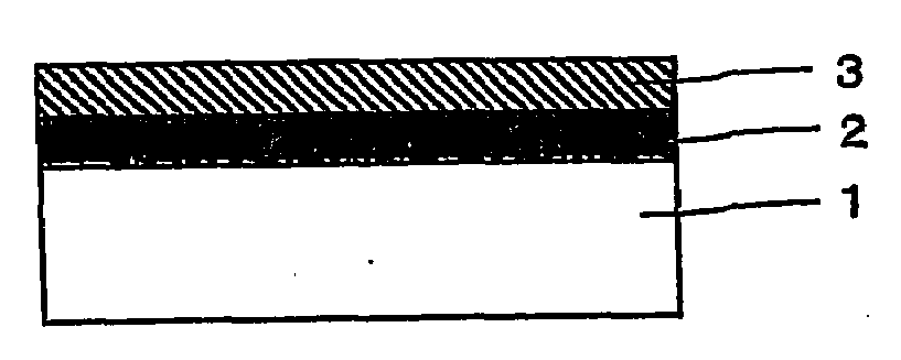
Transparent conductive film and method for production thereof
a technology of transparent conductive film and conductive layer, which is applied in the direction of conductive layer on the insulating support, non-metal conductors, instruments, etc., can solve the problems of degrading the resistance value or the moisture and heat resistance, and achieve the improvement of the crystallinity of the zno-based transparent conductive thin film 3, less mobile, and increased resistance
- Summary
- Abstract
- Description
- Claims
- Application Information
AI Technical Summary
Benefits of technology
Problems solved by technology
Method used
Image

Examples
examples
[0053]The invention is more specifically described with the examples below which are not intended to limit the scope of the invention.
examples 1
[0054]Organic Polymer Film Substrate
[0055]The organic polymer film substrate used was a polyethylene terephthalate (PET) film 0300E (100 μm in thickness) manufactured by Mitsubishi Plastics Inc.
[0056]Pretreatment
[0057]The PET film was attached to a winding system equipped with a plasma treatment unit, one dual-magnetron sputtering electrode, and two single-magnetron sputtering electrodes. Degassing was performed with an evacuation system including a cryocoil and a turbopump to produce an ultimate vacuum of 1.5×10⁻⁶ Pa, while the PET film was wound by means of a roller electrode heated at 120° C. Argon gas was then introduced, and the PET film was allowed to pass through plasma discharge at 13.56 MHz so that the smooth surface on which films were to be deposited was pretreated.
[0058]Formation of Aluminum Oxide Thin Film
[0059]A target of Al was then mounted on the dual magnetron sputtering electrode. While argon gas was introduced at 150 sccm (unit of air-equivalent gas flow rate), ox...
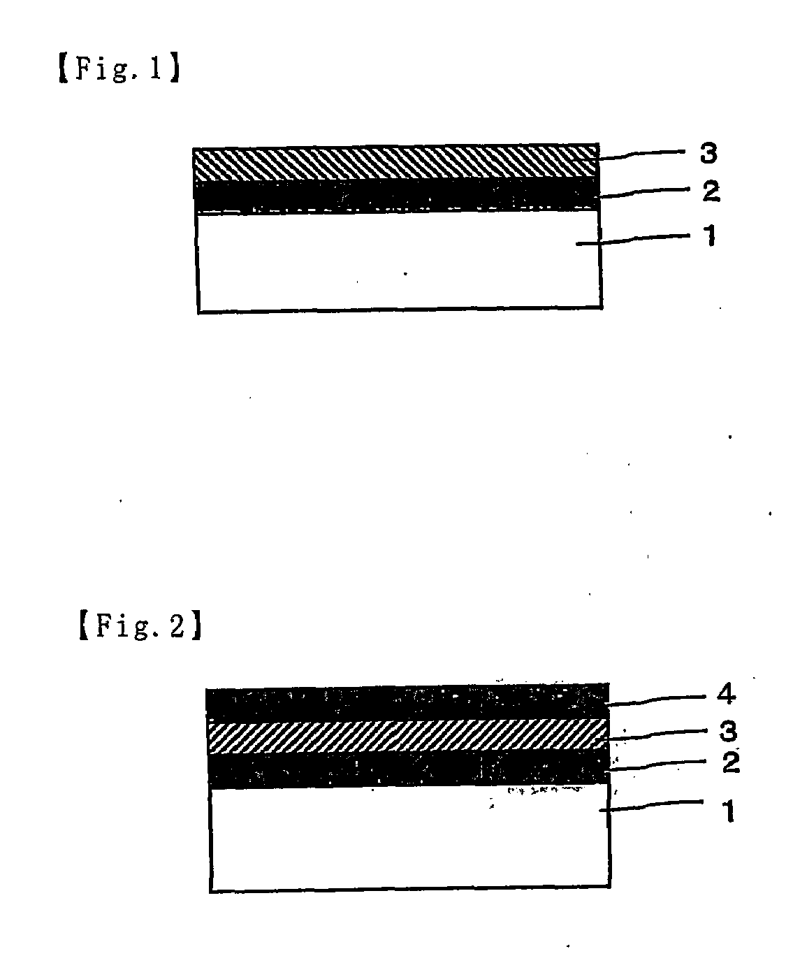
example 2
[0068]The process of Example 1 was performed until the GZO thin film was formed. Another aluminum oxide thin film (about 5 nm in thickness) was then formed as the second oxide thin film (overcoat layer) on the GZO thin film. The aluminum oxide thin film was formed by the same method as the undercoat layer in Example 1. The overcoat layer had a water-vapor transmission rate of 1.0 g / m2 per day or less as measured by MOCON method under the conditions of an atmosphere temperature of 40° C. and a relative humidity of 90%. In each example below using an overcoat layer, the second oxide thin film used had a water-vapor transmission rate of 1.0 g / m2 per day or less.
PUM
| Property | Measurement | Unit |
|---|---|---|
| temperature | aaaaa | aaaaa |
| thickness | aaaaa | aaaaa |
| thickness | aaaaa | aaaaa |
Abstract
Description
Claims
Application Information