Mos type semiconductor device

a semiconductor device and mos-type technology, applied in the direction of semiconductor devices, basic electric elements, electrical appliances, etc., can solve the problems of reducing the withstand voltage or increasing the leakage current, changing the characteristic of the mos-type semiconductor device, and lowering the withstand voltage. the effect of improving the radiation resistan

Inactive Publication Date: 2009-12-17
FUJI ELECTRIC CO LTD
View PDF8 Cites 8 Cited by
  • Summary
  • Abstract
  • Description
  • Claims
  • Application Information

AI Technical Summary

Benefits of technology

[0036]The invention provides a MOS type semiconductor device with improved radiation resistance and increased withstand voltage. In accordance with the invention, an MOS type semiconductor device is provided that includes an insulating film disposed on a semiconductor substrate, and a thin film disposed on the insulating film so as to be lower in resistivity than the insulating film, wherein the thin film is electrically connected to a source electrode or to both the source electrode and a drain electrode. With this configuration, electric charges produced in the insulating film by radiation can be let out rapidly via the thin film and the source electrode.
[0038]The thin film is preferably disposed so that a source portion and a drain portion disposed on the semiconductor substrate to form the MOS type semiconductor device are surrounded by the thin film. In this manner, the source portion and the drain portion are surrounded by the thin film so that electric charges produced in the insulating film can be removed or fixed effectively.
[0043]According to the invention, an MOS type semiconductor device improved in radiation resistance can be achieved in such a manner that a separation structure portion of an MOSFET is formed as a three-layer structure in which: a LOCOS film or a thermal oxide film is provided as a first layer on a silicon interface, an electric charge easily-movable film (such as a semi-insulative thin film or a conductive thin film) is provided as a second layer and an insulating film (such as a BPSG film or a laminated film having an HTO film and a BPSG film) is provided as a third layer; and the second layer is connected to a source electrode to thereby suppress the amount of plus fixed electric charges stored in the silicon interface portion by irradiation with radiation.

Problems solved by technology

As a result, there occurs a change in characteristic of the MOS type semiconductor device such as reduction in withstand voltage or increase in leakage current.
Lowering of the withstand voltage is however unavoidable.
It is however difficult to produce a high withstand voltage MOS type semiconductor device by combining the thin oxide film and the BPSG film.
When the amount of radiation increases, it is further difficult to produce a high withstand voltage MOS type semiconductor device because electric charges produced by radiation are not trapped so that surface inversion causes a leak path.

Method used


Image

  • Mos type semiconductor device
  • Mos type semiconductor device
  • Mos type semiconductor device

Examples


first embodiment

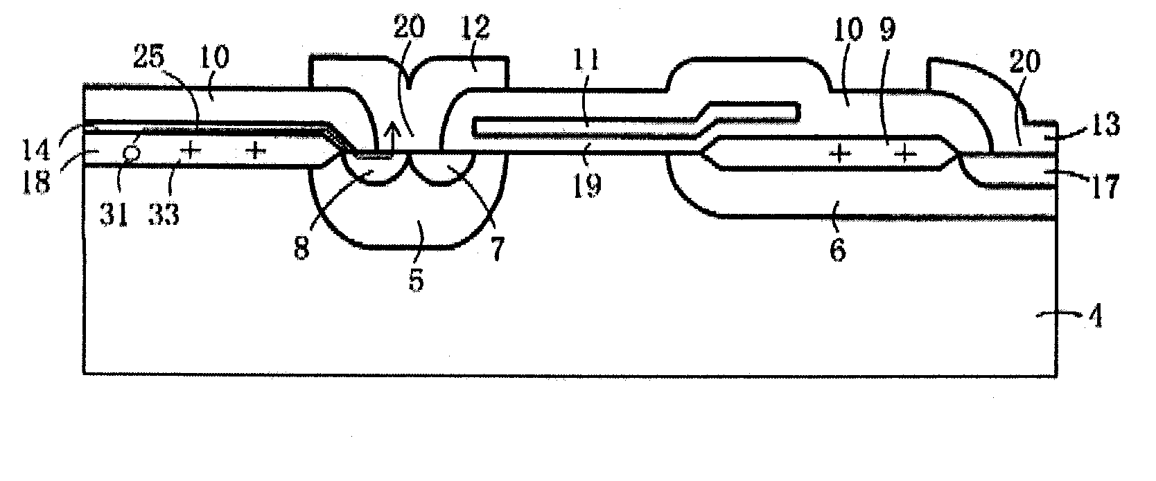
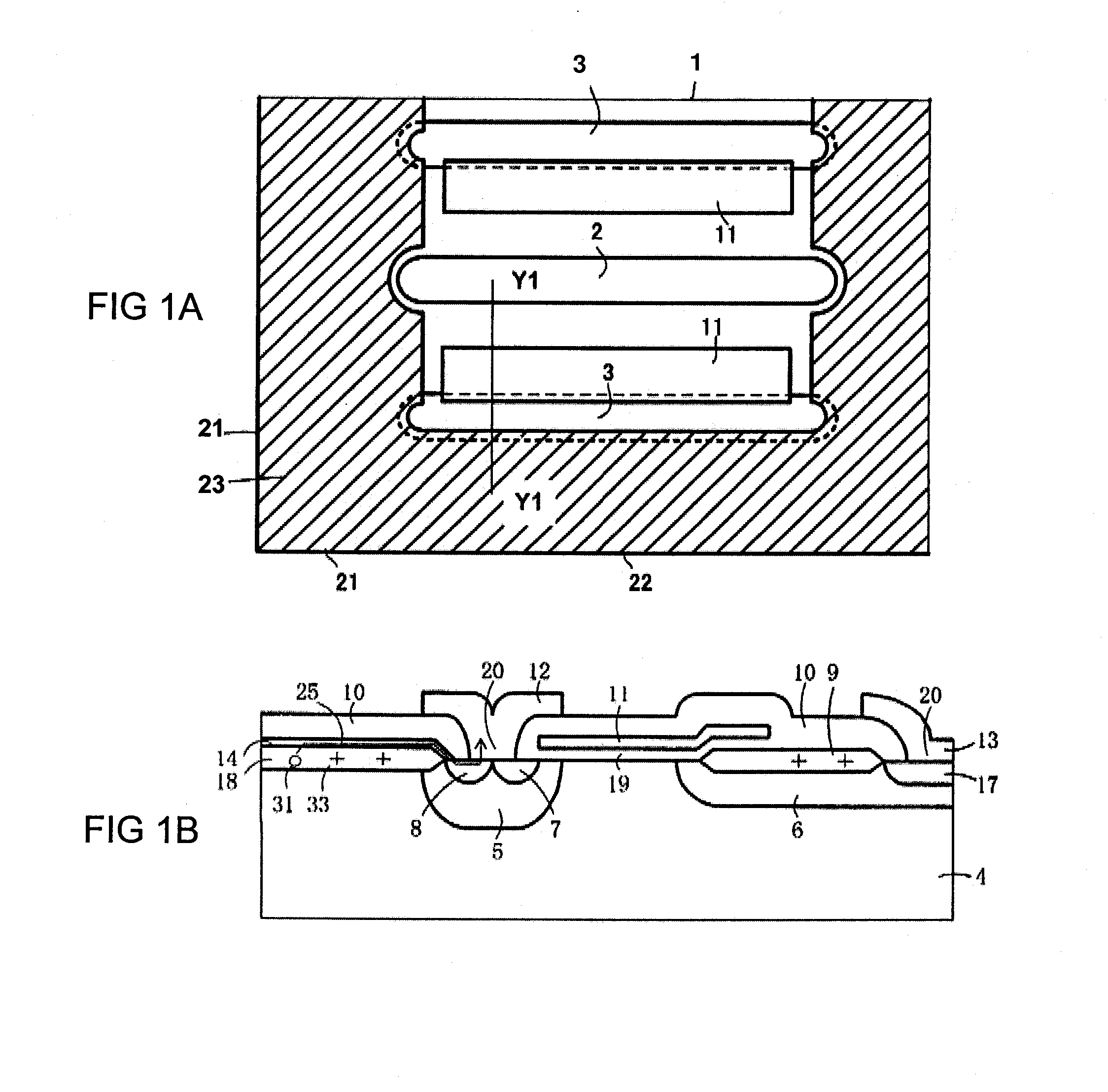
[0064]FIG. 1A is a plan view showing the configuration of important part of an MOS type semiconductor device according to the invention. FIG. 1B is a sectional view of important part, taken along the line Y1-Y1 in FIG. 1A. An MOSFET is taken as an example of the MOS type semiconductor device. The point of difference of this structure from the structure according to the background art lies in that a nitride film 14 is formed as a semi-insulative thin film on an LOCOS film 18 and electrically connected to a source electrode.

[0065]A low concentration p-type diffusion layer 5 (p-type well region) and a low concentration n-type diffusion layer 6 (n-type offset region) are formed in a surface layer of a p-type silicon substrate 4 so that the low concentration n-type diffusion layer 6 is disposed apart from the low concentration p-type diffusion layer 5. A high concentration-type diffusion layer 7 (n-type source region) and a high concentration p-type diffusion layer 8 (p-type contact regi...

second embodiment

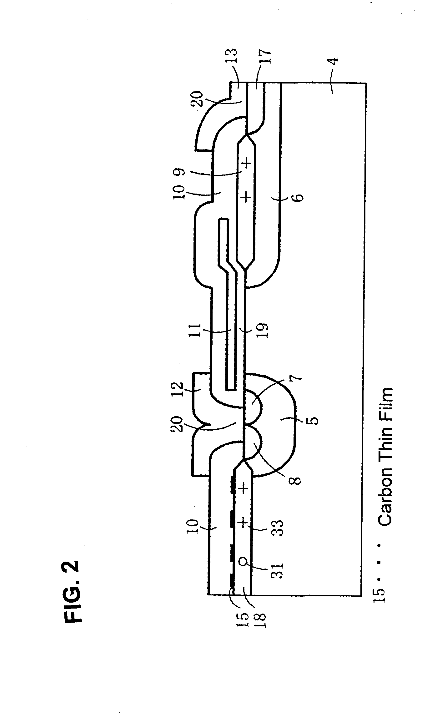
[0077]FIG. 2 is a sectional view showing important part of an MOS type semiconductor device according to the invention. A MOSFET is taken as an example of the MOS type semiconductor device. The point of difference of FIG. 2 from FIG. 1B lies in that a carbon thin film 15 is used in place of the nitride film 14. The carbon thin film 15, which is preferably a conductive thin film having an average thickness of 0.1 nm, is formed between the LOCOS film 18 and the BPSG film 10. In this embodiment, the withstand voltage drop is 15V which is improved compared with the background art. The level of the leakage current is the same as in the background art. In this embodiment, the carbon thin film 15 is preferably formed by a sputtering method so that the average thickness of the carbon thin film 15 is 0.5 nm. Besides carbon, a high melting point metal such as tungsten, titanium or chromium may be used.

[0078]Because this type metal generally shows poor wetability with the LOCOS film 18, this t...

third embodiment

[0083]FIG. 3 is a sectional view showing important part of an MOS type semiconductor device according to the invention. A MOSFET is taken as an example of the MOS type semiconductor device. The point of difference of FIG. 3 from FIG. 1B lies in that an insulative thin film for producing minus fixed electric field, such as an HTO (High Temperature Oxide) film 16, is used as an intermediate layer in place of the nitride film 14. Minus fixed electric field is produced under the presence of minus fixed electric charges 32 in the HTO film 16.

[0084]In this embodiment, the HTO film 16 which is an insulative thin film about 0.2 μm thick is formed between the LOCOS film 18 and the BPSG film 10. Because the HTO film 16 is apt to be negatively electrically charged after film-formation, minus fixed electric charges 32 can exist in the HTO film 16. As a result, fixed electric charges in the silicon interface made of a combination of the LOCOS film 18, the HTO film 16 and the BPSG film 10 can be ...


PUM

PropertyMeasurementUnit
currentaaaaaaaaaa
refractive indexaaaaaaaaaa
thicknessaaaaaaaaaa

Abstract

A MOS type semiconductor device, in which both improvement in radiation resistance and increase in withstand voltage is achieved, includes a nitride film formed on a LOCOS film and a PBSG film formed on the nitride film. The refractive index of the nitride film is set in a range of from 2.0 to 2.1 and the thickness of the nitride film is set in a range of from 0.1 Am to 0.5 μm to thereby provide the nitride film as a semi-insulative thin film. Of electron-hole pairs produced in the LOCOS film by γ-ray irradiation, holes low in mobility are let away to a source electrode via the nitride film to thereby suppress the amount of plus fixed electric charges stored in the LOCOS film. The provision of such a three-layer structure permits improvement in radiation resistance and increase in withstand voltage.

Description

BACKGROUND OF THE INVENTION[0001]The present invention relates to an MOS type semiconductor device improved in radiation resistance.[0002]A thick separation oxide film is generally provided for element separation in an MOS type semiconductor device. An oxide film called “field oxide film”, for example, about 1 μm thick is formed in the periphery of an active portion of an element in which a main electric current flows. Generally, each of the field oxide film and the thick separation oxide film is made of an oxide film (hereinafter referred to as “LOCOS film”) formed by an LOCOS (Local Oxidation of Silicon) technique.[0003]When such an MOS type semiconductor device is irradiated with an ionizing radiation such as a gamma (γ) ray, electron-hole pairs are produced in the LOCOS film or a gate oxide film. When a voltage is applied to the MOS type semiconductor device, the produced electrons move toward a plus electrode (drain electrode side) and the produced holes move toward a minus ele...

Claims


Application Information

Patent Timeline
Patent Type & Authority Applications(United States)
IPC IPC(8): H01L29/78
CPCH01L29/0649H01L29/1083H01L2924/0002H01L29/7835H01L2924/00
Inventor WATANABE, YASUMASA
Owner FUJI ELECTRIC CO LTD
Why Eureka
Try Eureka