Amplifier compression adjustment circuit

a compression adjustment and amplifier technology, applied in the direction of amplifier details, differential amplifiers, amplifiers with semiconductor devices/discharge tubes, etc., can solve the problems of /b> sacrificing more efficiency, undesirable wide spectral occupancy, power waste during the off-peak of amplitude, etc., to achieve narrower bandwidth, significantly sacrificing efficiency, and different levels of efficiency

Active Publication Date: 2010-08-05
QUANTANCE
View PDF58 Cites 28 Cited by
  • Summary
  • Abstract
  • Description
  • Claims
  • Application Information

AI Technical Summary

Benefits of technology

[0016]In a second embodiment of the present invention, the amplitude correction signal is split into two or more signals with different frequency ranges and provided respectively to different types of power supplies with different levels of efficiency to generate the adjusted supply voltage provided to the power amplifier. For example, in the second embodiment, the power supplies include a first power supply with a first efficiency and a second power supply with a second efficiency higher than the first efficiency. The first power supply receives a first portion of the amplitude correction signal in a first frequency range and generates a first adjusted supply output based upon the first portion of the amplitude correction signal, and the second power supply receives a second portion of the amplitude correction signal in a second frequency range lower than the first frequency range and generates a second adjusted supply output based upon the second portion of the amplitude correction signal. The first and second adjusted supply outputs are combined to form the adjusted supply voltage provided to the power amplifier. The first power supply can be a linear regulator, and the second power supply can be a switched mode power supply. By dividing the amplitude correction signal into two or more signals with different frequency ranges, the second embodiment of the present invention has the additional advantage that the switched mode power supply may be implemented with even narrower bandwidth as compared to the first embodiment without significantly sacrificing efficiency. A narrower bandwidth power supply or a variable power supply with a smaller range of voltage variation is easier to implement.
[0017]In a third embodiment of the present invention, the amplitude control loop further comprises a gain control module receiving the amplitude correction signal to generate a gain control signal, and a variable gain amplifier adjusting the amplitude of the input signal according to the gain control signal. The third embodiment has the advantage that it is possible to operate the power amplifier at any given depth beyond its compression point, resulting in an extra degree of freedom in designing the PA circuit. This is useful in optimizing the efficiency gain versus spectral

Problems solved by technology

RF PAs are one of the most significant sources of power consumption in these electronic devices, and their efficiency has a significant impact on the battery life on these portable electronic devices.
Since the RF spectrum is shared amongst users of the cellular telephone, a wide spectral occupancy is undesirable.
This typically results in power being wasted during the off-peak of the amplitude of the RF input signal 106, as the biasing remains fixed for the acceptable distortion at the peak power level.
Certain RF modulation techniques have evolved to require even more spectral efficiency, and thereby forcing the RF PA 104 to sacrifice more efficiency.
However, the EER technique often fails to provide significant efficiency gains, because the supply voltage 108 cannot be varied in an energy-efficient way to accommodate the large variations in the amplitude signal of the RF input signal 106 and thus it fails to provide a substantial energy efficiency gain while maintaining the required linear amplification of the RF signal in the RF PA 104.
This is mainly due to the difficulty in realizing a fast, accurate, wide range, and energy efficient voltage converter to drive the supply voltage of the RF PA 104.
This results in no change in the overall battery power being consumed by the RF transmitter, because any efficiency gained in the RF PA 104 is mostly lost in

Method used


Image

  • Amplifier compression adjustment circuit
  • Amplifier compression adjustment circuit
  • Amplifier compression adjustment circuit

Examples


first embodiment

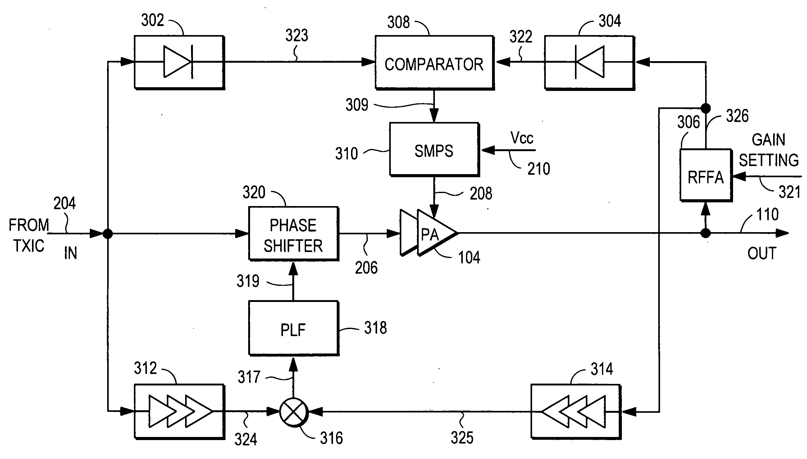
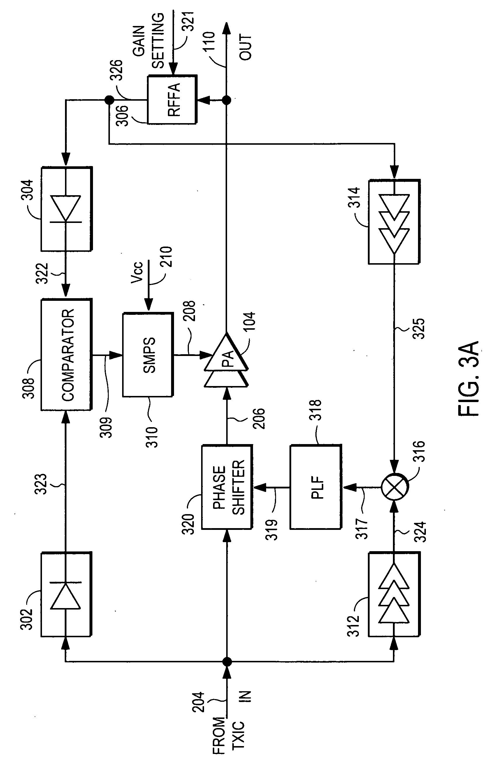
[0046]FIG. 3A illustrates an RF PA system, according to the present invention. The RF PA system includes the PA 104, and the PA controller 202 including a closed amplitude control loop and a closed phase control loop.

[0047]The phase control loop includes two limiters 312, 314, a phase comparator 316, a loop filter (PLF (Phase Loop Filter)) 318, and a phase shifter 320. To achieve stability over all conditions, the phase comparator 316 is of an adequate type with a capture range greater than 2*PI. To achieve this, a combination of adjustable delay elements and frequency dividers may be used. Also a phase sub-ranging system can be used since the dynamic phase variations that the phase correction loop processes are limited in amplitude. A sub-ranging phase control block (not shown) could be one of the constituents of the phase comparator 316 used with this system. Advantages of using sub-ranging in the phase comparator 316 are stability and good noise.

[0048]The amplitude control loop i...

second embodiment

[0059]FIG. 4A illustrates an RF PA system, according to the present invention. The RF PA system illustrated in FIG. 4A is substantially the same as the RF transmitter circuit illustrated in FIG. 3A, except that (i) the amplitude correction signal 309 is split into two signals, a high frequency amplitude correction signal 401 that is fed into a high frequency path including a linear regulator 402 and a low frequency amplitude correction signal 403 that is fed into a low frequency path including an SMPS 404 and that (ii) the outputs of the linear regulator 402 and the SMPS 404 are combined in the adder block406 to generate the adjusted supply voltage 208 to the PA 104. For example, a simple current adding node, a small, high frequency transformer or other types of active electronic solutions can be used as the adder block 406. Any other types of power combiner circuits may be used as the adder block 406. The high frequency amplitude correction signal 401 is input to the linear regulat...

third embodiment

[0072]In the embodiment of FIG. 5A, the independent programming of gain and compression point by the closed amplitude control loop also makes it possible to reduce the amount of high frequency energy that the power supply system (linear regulator) has to deliver to the PA 104. This can be done by having the variable gain amplifier 502 correct for some of the gain error at a higher speed than the Vcc control loop (closed on node 208) can do, thus reducing the amount of correction that is to be done by the low efficiency, high frequency branch (linear regulator 401). Thus, the bandwidth of the signals at nodes 208 and 504 can be made to be significantly different. Since only a small fraction of the energy resides at high frequencies, there is only a small penalty in efficiency for reducing the bandwidth of the control at node 208 relative to the bandwidth at node 504. The ratio of the two active bandwidths is part of the design trade-off for the whole system. The gain control block 50...


PUM


Abstract

An RF power amplifier system adjusts the supply voltage to the power amplifier based upon an amplitude correction signal indicating the amplitude difference between the amplitude of the RF input signal and an attenuated amplitude of the RF output signal of the power amplifier. A variable gain amplifier (VGA) adjusts the amplitude of the RF input signal, thus providing a second means of adjusting the amplitude of the output of the power amplifier. The gain of the VGA or the supply voltage to the power amplifier is controlled based on the AC components of the amplitude correction signal, while the DC components of the amplitude correction signal are blocked from controlling the VGA or the supply voltage to the power amplifier. The DC level of the gain control of the VGA, the average supply voltage to the power amplifier, or the closed loop gain of the overall amplitude correction loop is controlled separately by a compression control signal.

Description

BACKGROUND OF THE INVENTION[0001]1. Field of the Invention[0002]The present invention relates to a circuit for controlling RF PAs (Radio Frequency Power Amplifiers), and more specifically, to an RF PA controller circuit that controls the supply voltage of a PA using a closed amplitude control loop with an amplitude correction signal.[0003]2. Description of the Related Art[0004]RF (Radio Frequency) transmitters and RF power amplifiers are widely used in portable electronic devices such as cellular phones, laptop computers, and other electronic devices. RF transmitters and RF power amplifiers are used in these devices to amplify and transmit the RF signals remotely. RF PAs are one of the most significant sources of power consumption in these electronic devices, and their efficiency has a significant impact on the battery life on these portable electronic devices. For example, cellular telephone makers make great efforts to increase the efficiency of the RF PA systems, because the effi...

Claims


Application Information

Patent Timeline
IPC IPC(8): H03F3/45
CPCH03F1/0227H03F1/0238H03F1/0266H03F1/0272H03F1/3247H03F2200/99H03F3/24H03F2200/105H03F2200/408H03F2200/78H03F3/195
Inventor DROGI, SERGE FRANCOISVINAYAK, VIKAS
Owner QUANTANCE
Why Eureka
Try Eureka