Manufacturing method of a semiconductor element

a manufacturing method and semiconductor technology, applied in the field of manufacturing methods of semiconductor elements, can solve the problems of low production yield of semiconductor elements, difficult suffer from the manufacturing methods of the semiconductor elements described above, so as to reduce the manufacturing cost of semiconductor elements, and reduce the manufacturing cost

Inactive Publication Date: 2010-08-26
SUMITOMO ELECTRIC IND LTD
View PDF8 Cites 23 Cited by
  • Summary
  • Abstract
  • Description
  • Claims
  • Application Information

AI Technical Summary

Benefits of technology

[0018]In the above methods, the second film is used as the mask for forming the ridge portion, and the second film (having the top surface on which the portion of the protective film is formed) will be removed simultaneously with the removal of the first film for exposing the top surface of the ridge portion. Therefore, the portion of the protective film can be reliably removed from the top surface of the ridge portion. Accordingly, the possibility that the position of the top surface of the ridge portion deviates from the position of the portion of the protective film to be removed can be small, as compared with the case where a new resist pattern or the like independent of the mask used for forming the ridge portion is formed for removing the portion of the protective film from the top surface of the ridge portion. Accordingly, it is possible to prevent occurrence of such a problem that the position of the top surface of the ridge portion (i.e., the position where the electrode is formed) deviates from the position of the portion from which the protective film is removed, and thereby the position of the exposed portion of the electrode deviates from the designed position so that characteristics of the semiconductor element deteriorates or an operation failure occurs. Consequently, it is possible to suppress the increase in manufacturing cost due to the lowering of the manufacturing yield of the semiconductor element.
[0019]Further, in the step of forming the ridge portion after forming the electrode layer, the electrode layer is etched to have the same planar form as the ridge portion. Therefore, it is possible to reduce the possibility that the top surface (i.e., the surface in contact with the electrode layer) of the ridge portion is oxidized or contaminated by impurities in the step of forming the ridge portion and other steps. Consequently,

Problems solved by technology

The conventional manufacturing methods of the semiconductor elements described above suffer from the following problems.
In this processing, however, the portion of the second protective film may not be removed completely from the top surface of the ridge portion so that the second protective film may be left as burrs.
In this case, when the electrode is formed on the top surface of the ridge portion, contact between the top surface of the ridge portion and the electrode may be incomplete, resulting in a low production yield of the semiconductor element.
In this case, it is difficult to reduce the manufacturing cost of the semiconductor element.
However, adjustment of such positioning becomes more difficult as the size of the ridge portion decreases.
When the position of the mask pattern deviates from the position of the ridge portion, the position of the electrode will deviate from the position o

Method used


Image

  • Manufacturing method of a semiconductor element
  • Manufacturing method of a semiconductor element
  • Manufacturing method of a semiconductor element

Examples


first embodiment

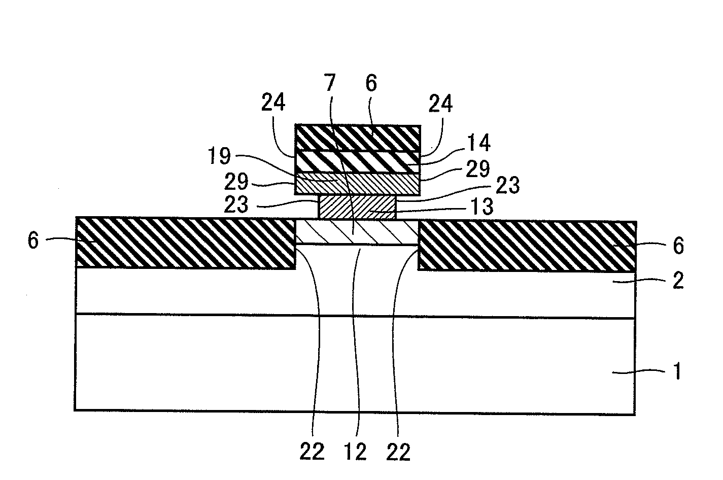
[0030]Referring to FIGS. 1 to 11, a manufacturing method of a compound semiconductor element according to the invention will be described below.

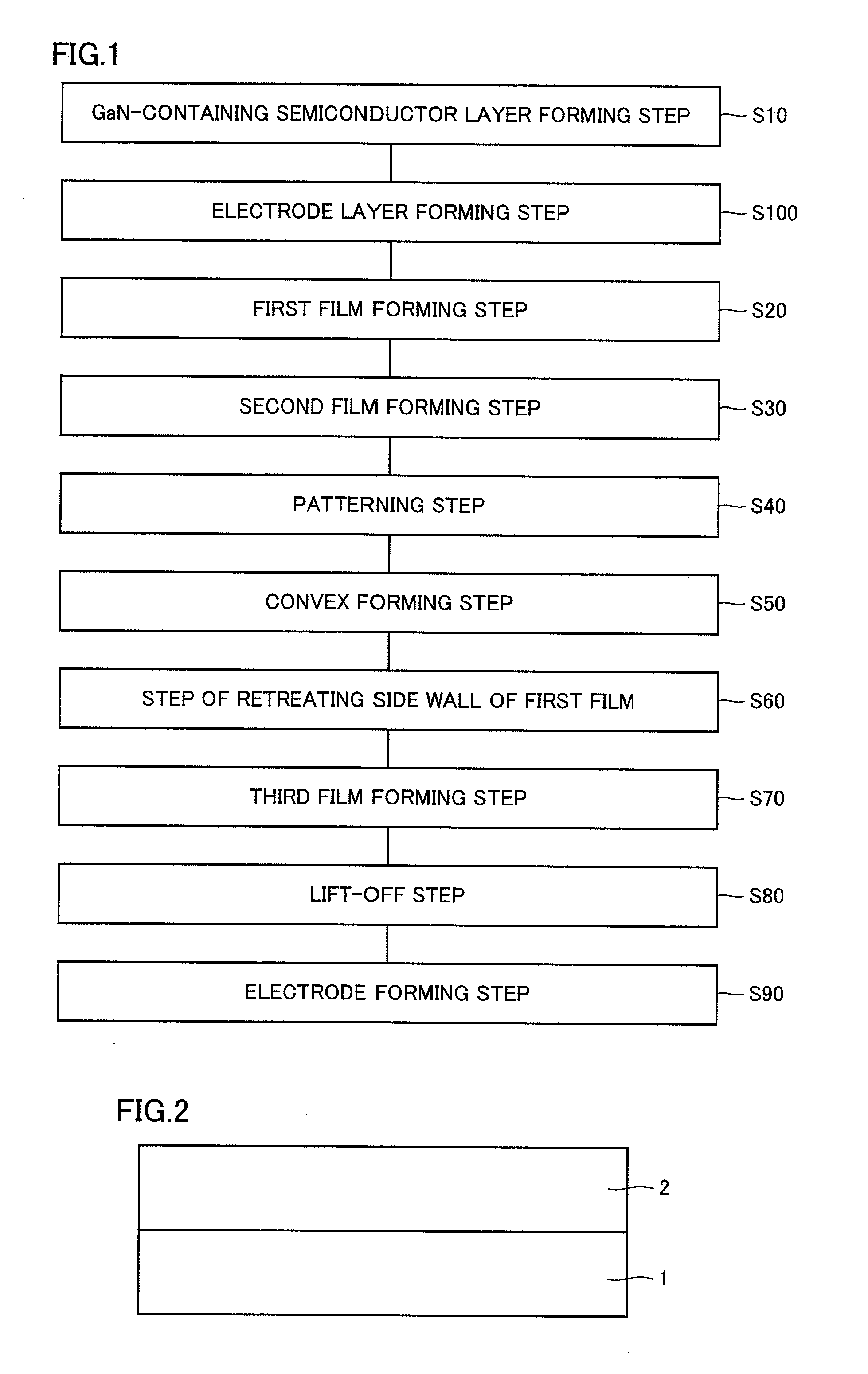
[0031]In the manufacturing method of the compound semiconductor element according to the invention, as shown in FIG. 1, a step (S10) of forming a GaN-containing semiconductor element is first executed. In this step (S10), as shown in FIG. 2, a GaN-containing semiconductor layer 2 is first formed on a main surface of a substrate 1 by an epitaxial growth method or the like. Substrate 1 may be made of, e.g., GaN, sapphire or the like which allows formation of a GaN-containing semiconductor layer on its main surface. GaN-containing semiconductor layer 2 may have a structure in which a plurality of GaN-containing semiconductor layers are layered according to required characteristics of the compound semiconductor layer to be formed. For example, when a semiconductor laser element is to be formed as the semiconductor element, and GaN-containing sem...

second embodiment

[0048]Referring to FIG. 12, a second embodiment of the manufacturing method of the compound semiconductor element according to the invention will be described below.

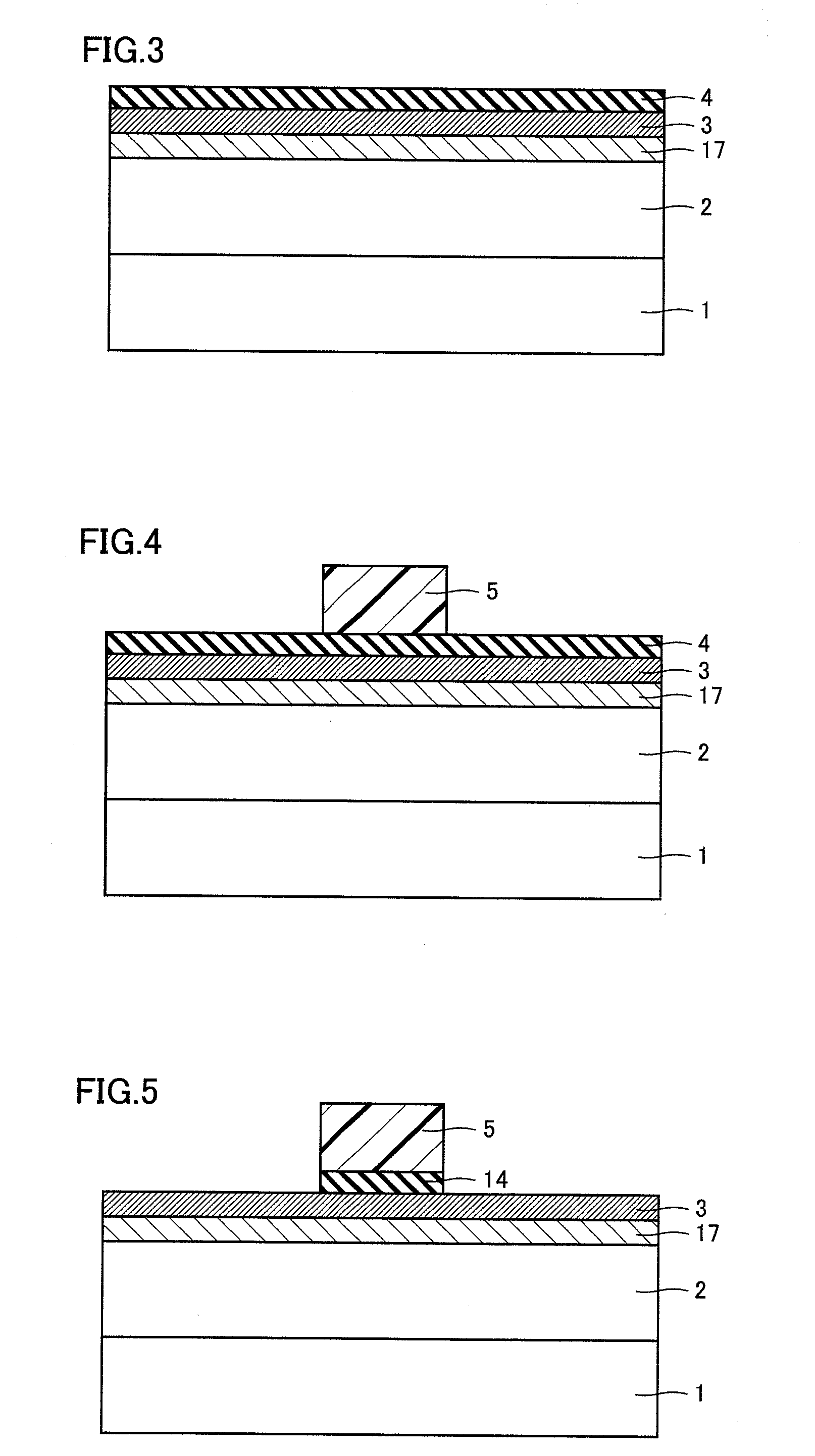
[0049]The second embodiment of the manufacturing method of the compound semiconductor element according to the invention basically includes substantially the same steps as the manufacturing method of the compound semiconductor element already described with reference to FIGS. 1 to 11 except for forming the layer used as a mask when forming ridge portion 12. More specifically, in the second embodiment of the manufacturing method of the compound semiconductor element according to the invention, steps (S10-S40) in the manufacturing method shown in FIG. 1 are first executed substantially in the same manner. Consequently, the structure shown in FIG. 4 is formed. Similarly to the case of the foregoing first embodiment, resist film 5 is used as the mask, and the RIE using a fluorine-containing etching gas is executed to remove ...

third embodiment

[0052]A third embodiment of the manufacturing method of the compound semiconductor element according to the invention basically has the same structure as the manufacturing method of the compound semiconductor element according to the invention shown in FIGS. 1 to 11, except for that the etchant used in the step (S60) of retreating the side wall of the first film and the lift-off step (S80) is not an alkaline solution but is a mixed acid made of phosphoric acid, nitric acid, acetic acid and water. The mixed acid may be a mixture of 80 wt. % of phosphoric acid, 5 wt. % of nitric acid, 10 wt. % of acetic acid and water. This can achieve substantially the same effect as the first embodiment of the invention.

[0053]In the case where the mixed acid is used as described above, mask layer 14 may likewise be made of a material other than SiO2, and it may be made of one of silicon oxide (SiO), silicon nitride (SiN), zirconium oxide (ZrO2), tantalum oxide (Ta2O3), lanthanum oxide (La2O5), ceric...


PUM


Abstract

A method of manufacturing a semiconductor element of good characteristics at a reduced manufacturing cost is provided. The manufacturing method of the semiconductor element includes a GaN-containing semiconductor layer forming step, an electrode layer forming step, a step of forming an Al film on the GaN-containing semiconductor layer, a step of forming a mask layer made of a material of which etching rate is smaller than that of a material of the Al film, a step of forming a ridge portion using the mask layer as a mask, a step of retreating a position of a side wall of the Al film with respect to a position of a side wall of the mask layer, a step of forming, on the side surface of the ridge portion and the top surface of the mask layer, a protective film made of a material of which etching rate is smaller than that of the material forming the Al film, and a step of removing the Al film and thereby removing the mask layer and a portion of the protective film formed on the top surface of the mask layer.

Description

BACKGROUND OF THE INVENTION[0001]1. Field of the Invention[0002]The present invention relates to a manufacturing method of a semiconductor element, and particularly to a method of manufacturing a semiconductor element having a gallium nitride-containing semiconductor layer.[0003]2. Description of the Background Art[0004]A semiconductor element having a ridge structure in a gallium nitride-containing semiconductor layer has been known. Various methods have been proposed for forming the ridge structure of the semiconductor element.[0005]For example, Japanese Patent Laying-Open No. 2000-004063 (which will be referred to as “patent document 1” hereinafter) has disclosed a technique in which a ridge structure is formed in a gallium nitride-containing semiconductor layer by dry etching, using a first protective film formed of a silicon oxide or a photoresist film as a mask. After the dry etching, a second protective film made of a material different from that of the first protective film ...

Claims


Application Information

Patent Timeline
IPC IPC(8): H01L21/00
CPCH01L21/32139H01L21/3081
Inventor KATAYAMA, KOJIKITABAYASHI, HIROYUKIARAKAWA, SATOSHI
Owner SUMITOMO ELECTRIC IND LTD
Why Eureka
Try Eureka