Energy conversion and energy storage devices and methods for making same

a technology of energy storage device and energy conversion device, which is applied in the direction of sustainable manufacturing/processing, measurement of semiconductor devices, and final product manufacturing, etc., can solve the problems of limited efficiency of solar energy conversion into electricity in pv devices, prohibitively expensive, and complex addition of junctions, etc., to achieve high aspect ratio, increase the efficiency of energy conversion device and energy storage device, and reduce the effect of thermalization loss

Active Publication Date: 2010-12-02
INTEGRATED DEVICE TECH INC
View PDF17 Cites 91 Cited by
  • Summary
  • Abstract
  • Description
  • Claims
  • Application Information

AI Technical Summary

Benefits of technology

[0027]Accordingly, it has been found that arrays of aligned material rods (e.g., material layers deposited within arrays of pore channels) having a relatively small diameter and a high aspect ratio may advantageously increase the efficiency of energy conversion devices and energy storage devices and may reduce losses in such devices. Further, the material rods may have reduced layer strain as compared to conventional thin film devices. Reduced strain between layers can reduce the number of dislocations in the material layers and

Problems solved by technology

One of the processes that limits the efficiency of the conversion of solar energy into electricity in PV devices is thermalization loss due to the electron-hole pair quickly losing energy to the creation of phonons.
While triple-junction solar cells have been developed with efficiencies approaching 30%, the required matching of lattice parameters and output current makes adding more junctions complex and prohibitively expensive.
Several challenges remain to making this a viable technology.
For example, most semiconductor materials are not durable in an aqueous environment, thus eliminating them as candidates for use in water-splitting.
Similarly, Group III-V semiconductors, such as the nitrides, are unstable in water and will rapidly oxidize.
TiO2 has excellent chemical stability when illuminated in an aqueous environment, and it has band edge energies well aligned with the H2 and O2 evolution reactions; however, its large band gap energy (3.0-3.2 eV) precludes absorption of most of the solar spectrum other than UV, thus limiting its efficiency.
Attempts at using other oxides with smaller band gaps have been largely unsuccessful.
However, iron has been shown to leach from the surface over time and the material therefore corrodes.
While recent advances in WO3 production show promise, its band gap energy of 2.6 eV is too large for efficient hydrogen production.
Beyond their large band gaps, one of the key limitations to using oxide semiconductors such as TiO2 for photoelectrochemical materials are losses related to the short exc

Method used


Image

  • Energy conversion and energy storage devices and methods for making same
  • Energy conversion and energy storage devices and methods for making same
  • Energy conversion and energy storage devices and methods for making same

Examples


example 1

Blank Nanoporous Support Member

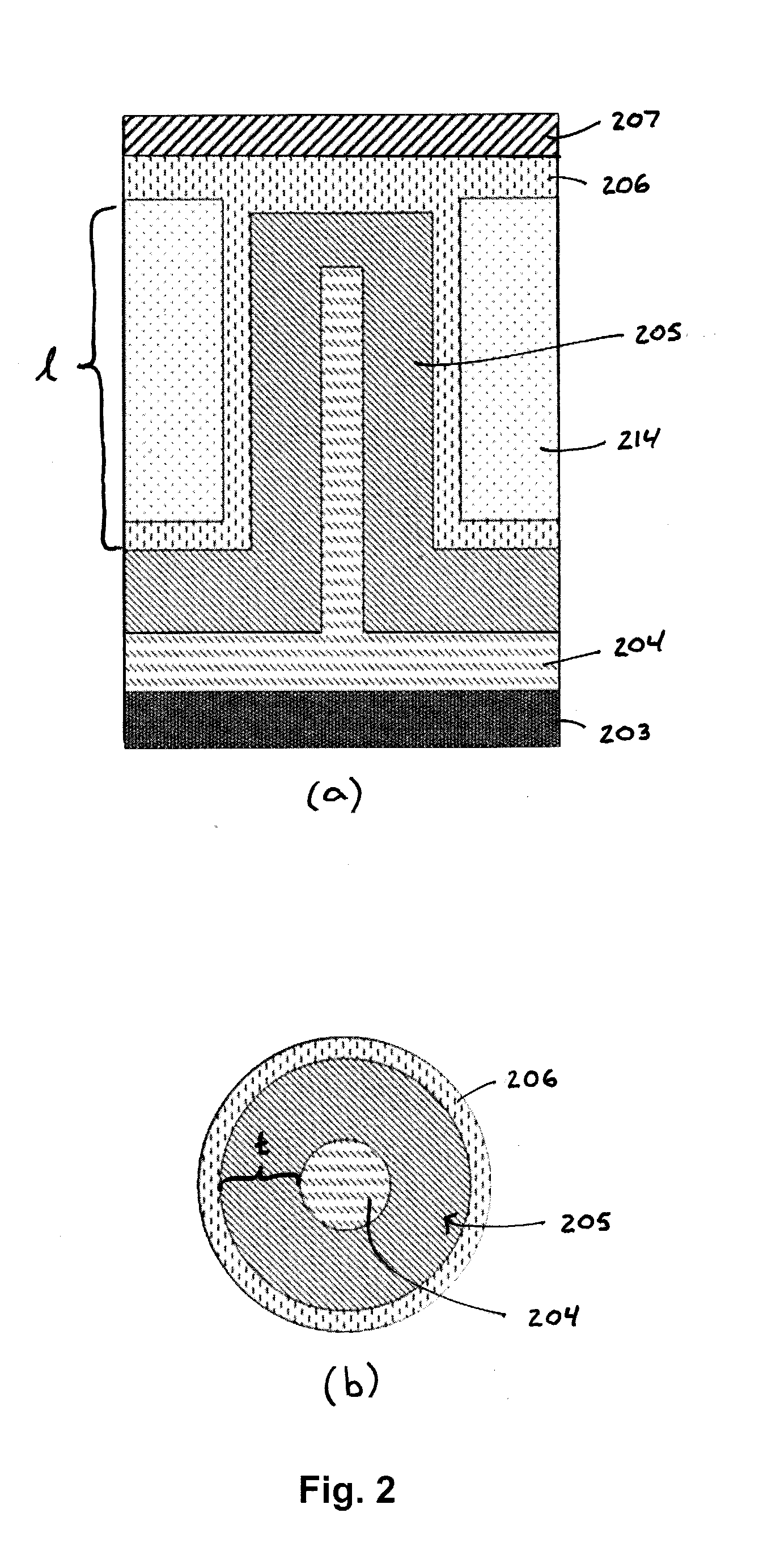
[0122]Blank nanoporous anodic aluminum oxide (AAO) support members are prepared in-part as described in U.S. Pat. No. 6,705,152 and U.S. Patent Publication No. 2007 / 0256562, which are each incorporated herein by reference in its entirety. In this example, AAO is formed using at least 98% pure Al foil. Optionally, prior to anodization, the foil can be rolled and pressure-annealed at about 350° C. and 5,000 psi for 20 min to improve its surface quality, achieve required thickness and reduce stress in the finished AAO support member. Al foil is anodized on both sides in 1% oxalic acid electrolyte at a temperature of 2° C. and anodization voltage of 100V (and as high as 300-400V in different electrolytes), until a charge density of about 2° C. / cm2 is accumulated, to form a sacrificial AAO layer. The sacrificial AAO layer can improve surface quality and pore channel ordering in the final AAO support member.

[0123]The resulting sacrificial layer of about 10 μ...

example 2

Arrays of Conductor Layers

[0128]Free-standing porous AAO support members are prepared as described in Example 1. Conductive material layers are grown by deposition of Al2O3-doped ZnO inside the pore channels using an atomic layer deposition (ALD) reactor. The ALD reactor is evacuated to less than 100 mTorr and heated to 110° C. and alternating gasses are injected into the ALD reactor.

[0129]In this regard, alumina is deposited on a free-standing 13 mm AAO support member by injecting trimethylaluminum (TMA) into the statically sealed ALD reactor to a total pressure of about 1 torr and holding it over the AAO substrates for 2 minutes. Then the gate valve is opened and the TMA is evacuated from the ALD reactor. After evacuation, ultrapure nitrogen is flowed through the reactor for 30 seconds and subsequently evacuated again to ensure removal of all unreacted TMA. The reactor is then filled with about 1 torr of water for 2 minutes, and is subsequently evacuated and again purged with nitr...

example 3

Coaxial Array Capacitor

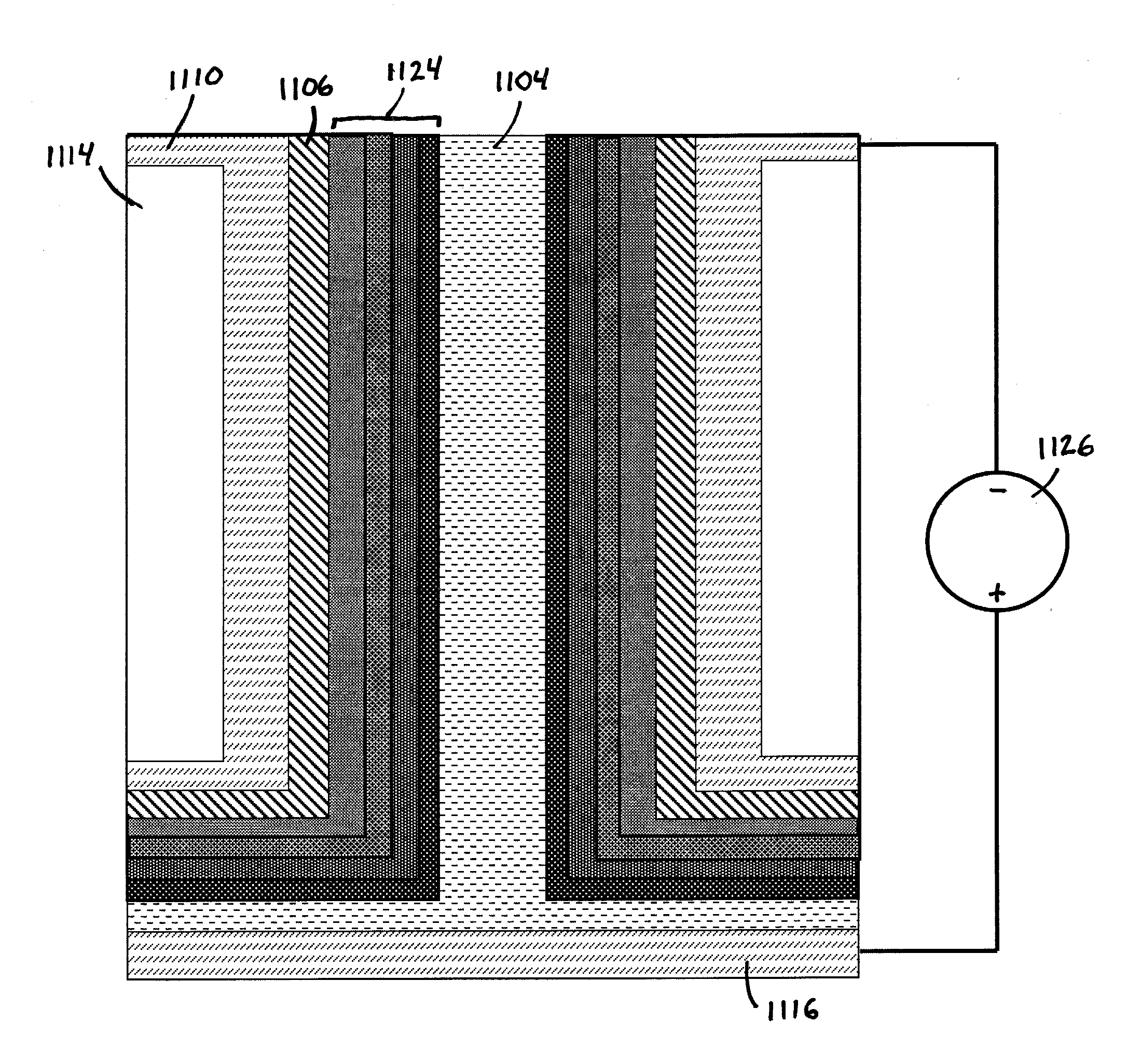
[0131]A capacitor is formed by sequential deposition of coaxial conductive and dielectric material layers inside the pore channels of AAO. Conductive material arrays are prepared as described in Example 1. Conductive material layers with a wall thickness of about 19 nm are prepared by repeating the 17 cycles of ZnO plus 1 cycle of alumina sequence 6 times (see Example 2). A gold contact is sputtered on one side of the support member, and a conductive wire is attached using conductive epoxy.

[0132]A dielectric material is then deposited to form a dielectric material layer on top of the first conductive layer within the pore channels. Alumina is used as the dielectric material, which is deposited in the same manner as the alumina deposition described in Example 2. By depositing 50 cycles of alumina, a material layer of ˜6 nm thickness is deposited. To form a second conductive layer to complete the capacitor structure, another deposition of a conductive Al2O3-dope...


PUM

PropertyMeasurementUnit
Lengthaaaaaaaaaa
Lengthaaaaaaaaaa
Lengthaaaaaaaaaa

Abstract

Energy devices such as energy conversion devices and energy storage devices and methods for the manufacture of such devices. The devices include a support member having an array of pore channels having a small average pore channel diameter and having a pore channel length. Material layers that may include energy conversion materials and conductive materials are coaxially disposed within the pore channels to form material rods having a relatively small cross-section and a relatively long length. By varying the structure of the materials in the pore channels, various energy devices can be fabricated, such as photovoltaic (PV) devices, radiation detectors, capacitors, batteries and the like.

Description

CROSS-REFERENCE TO RELATED APPLICATIONS[0001]This application claims priority to U.S. Provisional Patent Application Ser. No. 61 / 174,577 filed on May 1, 2009, which is incorporated herein by reference in its entirety.STATEMENT REGARDING FEDERALLY-FUNDED RESEARCH[0002]This invention was funded by the National Science Foundation under Grant No. IIP-0638104, by the Department of Energy under Grant No. DE-FG02-07ER84871, and by the Department of Homeland Defense under Grant No. HSHQDC-07-C-00113 all administered by the Small Business Innovation Research (SBIR) program. The Government has certain rights in this invention.BACKGROUND OF THE INVENTION[0003]1. Field of the Invention[0004]The present invention relates to the field of energy devices, such as energy conversion devices and energy storage devices. The devices can include a porous support member having pore channels, and one or more active material layers coaxially disposed within the pore channels. The devices can be utilized in ...

Claims


Application Information

Patent Timeline
IPC IPC(8): H01M10/00H01L31/02B01J19/08B05D5/12H01L31/0352H01L33/06
CPCC01B3/042G01T1/24G01T3/08H01L31/035281H01L31/115H01L33/24H01L51/0037H01L51/4213H01M6/40H01M8/1097H01M10/0436Y02E60/364H01L33/18Y02E10/549H01L2924/0002H01L2924/00Y02P70/56Y02P20/135Y02E60/36Y02P20/133Y02P70/50Y02E60/50Y02E60/10H10K85/1135H10K30/10
Inventor ROUTKEVITCH, DMITRIWIND, RIKARD A.
Owner INTEGRATED DEVICE TECH INC
Why Eureka
Try Eureka