

Nitrogen oxide sensitive field effect transistors for explosive detection comprising functionalized non-oxidized silicon nanowires
a technology of functionalized non-oxidized silicon nanowires and transistors, which is applied in the direction of instruments, electric/magnetic computing, analogue computers, etc., can solve the problems of limited application of these sensors, affecting the response of sensors based on oxide coatings, and limiting the effect of gate voltage on the transconductance
- Summary
- Abstract
- Description
- Claims
- Application Information
AI Technical Summary
Benefits of technology
Problems solved by technology
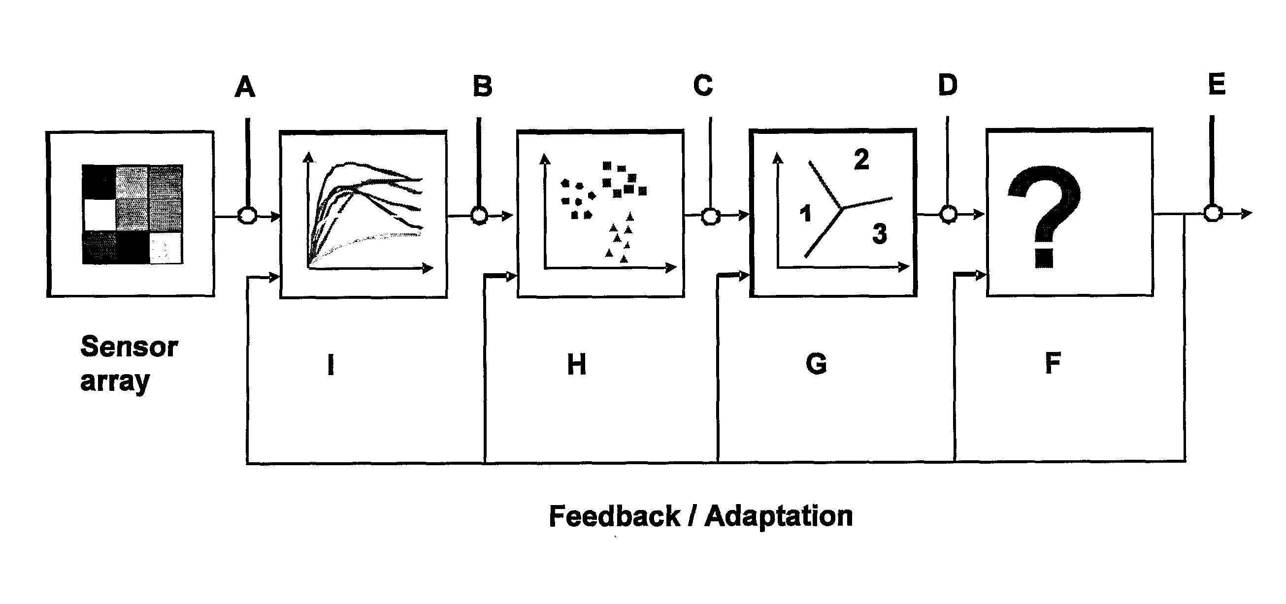
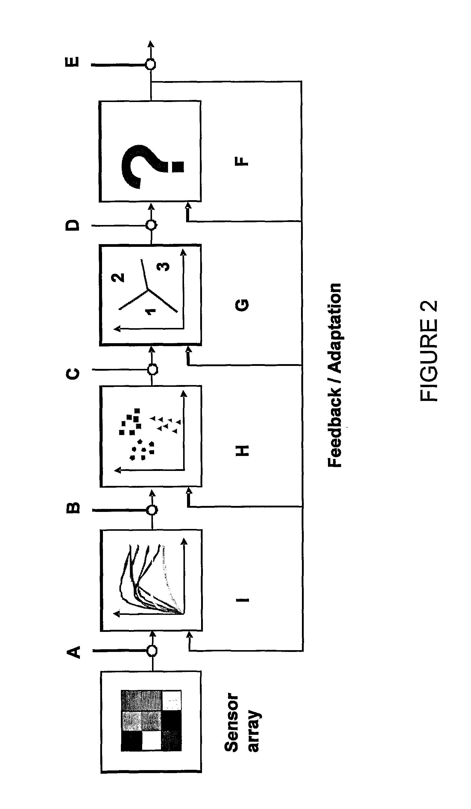
Method used
Image

Examples
example 1
Synthesis of the Silicon Nanowires (Si NWs)
[0093]The synthesis of Si NWs was performed as described in WO 2009 / 013754 which is incorporated herein by reference in its entirety. In particular, Si NWs were prepared by the vapor-liquid-solid (VLS) growth method using chemical vapor deposition (CVD) with silane on Si(111) substrates. Si substrates were etched in diluted HF to remove the native oxide following by sputtering of a 2 nm thick Au film on the substrate. The sample was transferred into the CVD chamber, and annealed at ˜580° C. with a pressure of ˜5×10⁻⁷ mbar for 10 minutes. The temperature was then dropped to ˜520° C. and a mixture of 5-10 sccm Ar and 5 sccm SiH4 was introduced for 20 minutes at a pressure of 0.5-2 mbar to obtained undoped Si NWs.
[0094]Doped Si NWs were prepared by the vapor-liquid-solid (VLS) growth technique under gas ratios of 10 seem He, 5 seem SiH4, and 0.02 seem B2H6 (2% in He), yielding p-type Si NWs doped with Boron. TEM characterization indicated that...
example 2
Functionalization of Si Nanowires (Si NWs)
[0095]The functionalization of the Si NWs was performed as described in WO 2009 / 013754 which is incorporated herein by reference in its entirety. In particular, functionalization of the Si NWs of the present invention was performed using a two-step chlorination / alkylation route. Prior to any chemical treatment, each sample was cleaned using a nitrogen (N2(g)) flow. Hydrogen-terminated Si NWs were then prepared by etching the amorphous SiO2 coating. This was done through exposing the Si NWs to buffered HF solution (pH=5) for 60 seconds followed by exposure to NH4F for 30 seconds. It is noteworthy that longer exposures to HF and / or NH4F results in fluorination of the sample thus interfering with the alkylation process. The sample was then removed and rinsed in water for 2(g) flow for 10 seconds. The sample was transferred into a glove-box with N2(g)-atmosphere for functionalization.
[0096]Functionalization was preformed by immersing the sample ...
example 3
Fabrication of the Si NW Field Effect Transistors
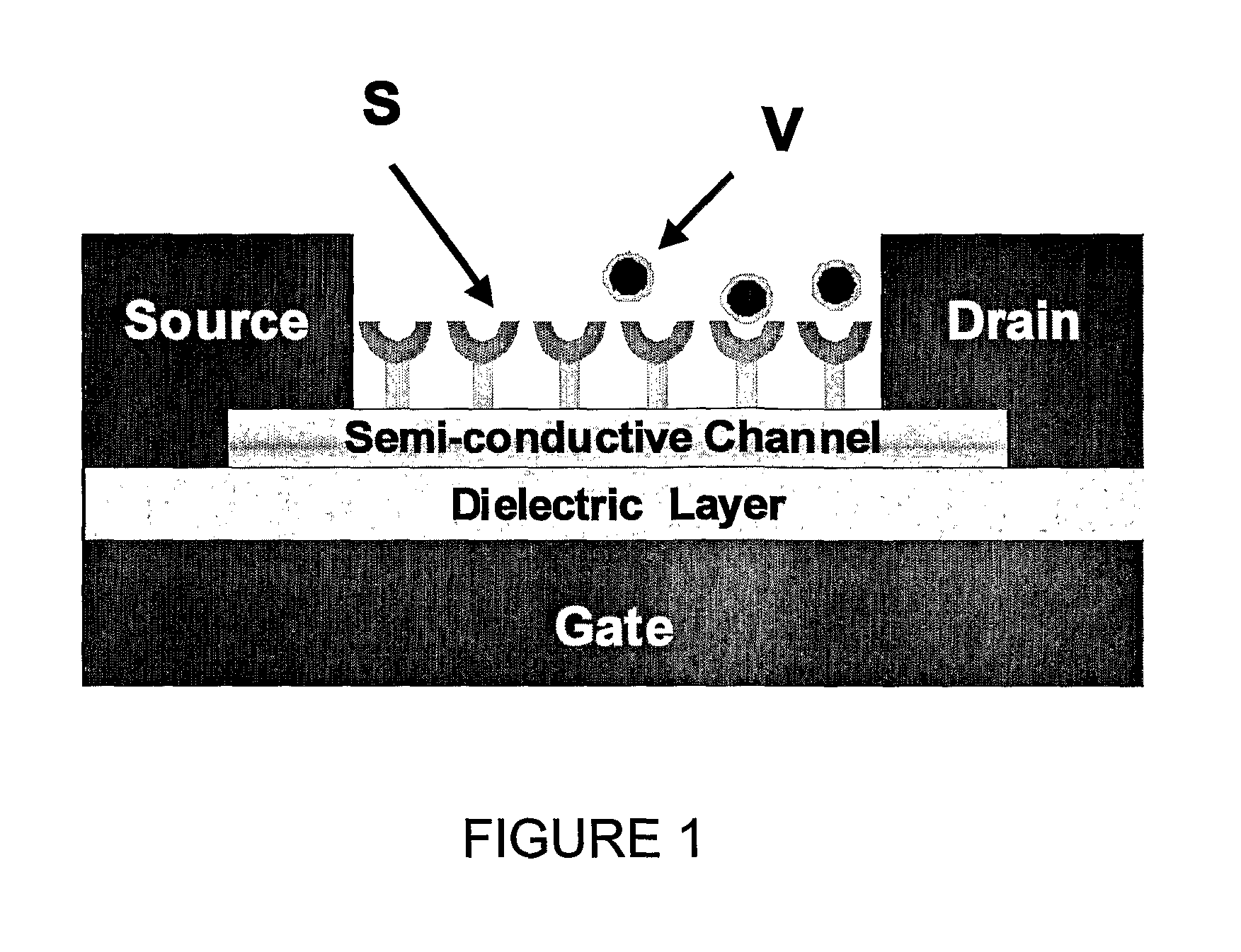
[0097]The fabrication of the Si NW FETs was performed as described in WO 2009 / 013754 which is incorporated herein by reference in its entirety. In particular, devices were fabricated by depositing four Al electrodes on an individual Si NW on top of a 90 nm thermally oxidized degenerately doped p-type Si (0.001 Ω·cm−1) substrate. The electrodes were mutually separated by 1.70±0.05 μm (FIG. 10). For each Si NW field effect transistor device, the intrinsic conductivity at determined back gate voltage was obtained by the four-point probe method. Particularly, electrical properties collected with the four-point probe method enable the configuration wherein there is no contact resistance between the metallic contacts and the Si NW.
PUM
 Abstract
Description
Claims
Application Information