Magnetization control method, information storage method, information storage element, and magnetic function element

a control method and information storage technology, applied in the field of information storage method, information storage element, and magnetic function element, can solve the problems of low writing speed in the s order, low rewriting frequency, high possibility, etc., and achieve the effect of increasing writing current and low power consumption

Inactive Publication Date: 2011-03-03
OSAKA UNIV
View PDF13 Cites 47 Cited by
  • Summary
  • Abstract
  • Description
  • Claims
  • Application Information

AI Technical Summary

Benefits of technology

[0033]The present invention can control a magnetization direction without using a current-induced magnetic field and spin transfer torque. Furthermore, each independent element is capable of working as a random access magnetic memory including an insulating layer for applying an electric field and a magnetic layer controlling anisotropy. Moreover, since the resistance value (gate resistance) between (i) a voltage application terminal for controlling a magnetization direction and (ii) an ultrathin film ferromagnetic layer can be increased significantly, the present invention can provide a multiterminal magnetic function element (spin transistor) having no interference with an output circuit. The provision of such a multiterminal magnetic function element (i) solves problems in the conventional techniques such as an increase in writing current and items of concern such as fringing fields, and (ii) produces a non-volatile and frequently-rewritable magnetic random access memory with low power consumption, and a magnetic function element such as a spin transistor which contributes to a nonvolatile logic.

Problems solved by technology

However, since the flash memory works on the principle of charge injection, many problems have to be overcome in order for the flash memory to be a universal memory.
These problems include a low writing speed that is in the μs order, and a low rewriting frequency that is in the 106 range.
However, with regard to writing methods, there is a high possibility for increased power consumption when facing a large amount of data exceeding giga-bit levels, and this is perceived to be a problem.
However, this technique might not be able to handle a large amount of capacity, such as over giga-bit levels, because of the following problems: (i) a greater amount of current is required as the size of the magnetic element decreases; (ii) and a writing error develops in a magnetic element close to the target magnetic element due to a fringing field from a wire.
The spin transfer torque technique has caught attention as an encouraging writing technique for the next-generation MRAM; however, the critical current density required for writing is not sufficiently low enough at the moment.
Thus, unfortunately, the technique has not achieved a low power consumption capability which surpasses that of competing memories.
This technique is intended to be applied to a mass storage medium, such as a hard disk, and thus application to a magnetic random access memory is difficult.
The use of the electrolytes, however, makes a configuration of a magnetic random access memory difficult.
Under the existing conditions, unfortunately, the piezoelectric and electrostrictive material is short of fatigue resistance.

Method used


Image

  • Magnetization control method, information storage method, information storage element, and magnetic function element
  • Magnetization control method, information storage method, information storage element, and magnetic function element
  • Magnetization control method, information storage method, information storage element, and magnetic function element

Examples


embodiment 1

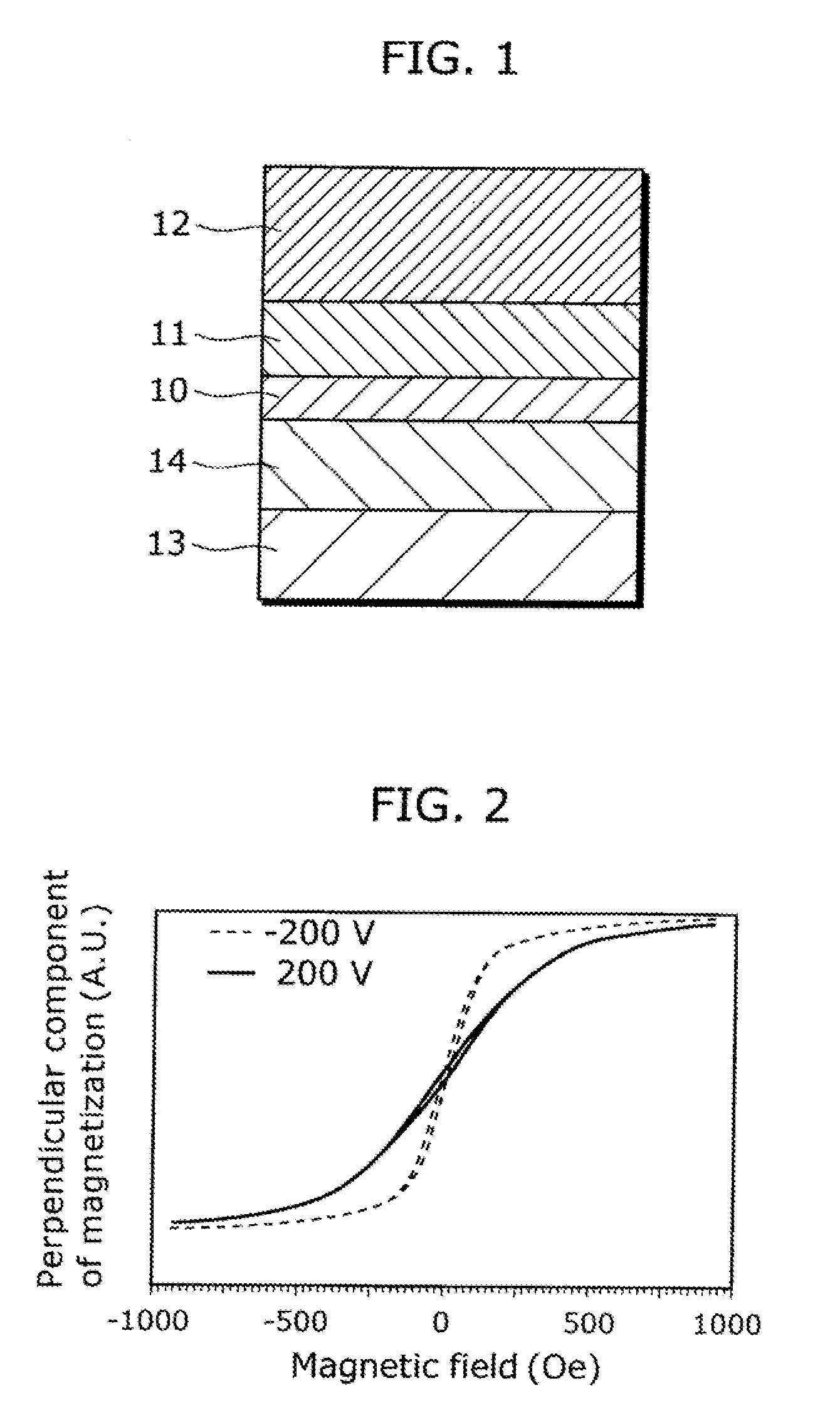
[0066]FIG. 1 is a cross-sectional view of a magnetic function element according to Embodiment 1 in the present invention.

[0067]In the magnetic function element, a magnetic layer 10, which is to be magnetically-controlled by having a voltage applied, is provided on a substrate 13 via a base layer 14; and an insulating layer 11, which works as a potential barrier, is provided in contact with the magnetic layer 10. Above the insulating layer 11, an electrode 12 is provided to apply a voltage to the magnetic layer 10.

[0068]The following substrates, for example, can be used as the substrate 13: a semiconductor substrate such as a silicon substrate, a plastic substrate, a glass substrate, a sapphire substrate, and a magnesium oxide substrate; and an insulating substrate.

[0069]The base layer 14 may be formed of: a layer made of (i) a noble metal including the following: gold (Au), silver (Ag), copper (Cu), aluminum (Al), chrome (Cr), and ruthenium (Ru), and (ii) a transition metal element;...

embodiment 2

[0093]FIG. 10 is a cross-sectional view of a magnetic function element according to Embodiment 2 in the present invention.

[0094]The magnetic function element has the magnetic layer 10 and the insulating layer 11 of Embodiment 1 switch their positions. The insulating layer 11, working as a potential barrier, is provided on the substrate 13 and the base layer 14. Here, the base layer 14 can be also used as a bottom electrode. On the insulating layer 11, the magnetic layer 10 is provided. Here, the magnetization reversal of the magnetic layer 10 is to be induced by an electric field. A voltage is applied between the electrode 12 provided on the magnetic layer 10 and the base layer 14.

[0095]As described above, the magnetic function element according to an implementation of the present invention includes a structure having: the magnetic layer 10 which is an ultrathin film ferromagnetic layer having a film thickness of one or more atomic layers and of 2 nm or less; and the insulating laye...

embodiment 3

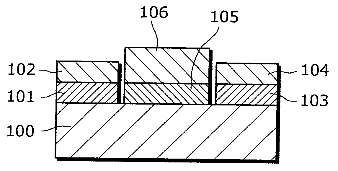
[0096]FIG. 11 is a cross-sectional view of a magnetic storage element (information storage element) according to Embodiment 3 in the present invention.

[0097]The magnetic storage element works as a single memory cell. The magnetic storage element is structured to have an extra magnetic layer (reference layer) 20 on the insulating layer 11 found in the magnetic function element according to Embodiment 1. A storage layer 21 is considered and structured in a similar manner (materials and film thickness) as the magnetic layer 10 in the magnetic function element according to Embodiment 1.

[0098]Including ferromagnetic metal, the reference layer 20 is sandwiched between the electrode 12 and the base layer 14, and stacked opposite the insulating layer 11 in relation to the storage layer 21. The reference layer 20 is made of the same material as the magnetic layer 10 is made. The magnetized state of the reference layer 20 remains fixed. Information is written by applying a voltage to control ...


PUM

PropertyMeasurementUnit
thicknessaaaaaaaaaa
voltageaaaaaaaaaa
coercive forceaaaaaaaaaa

Abstract

The present invention provides a magnetization control method controlling, utilizing no current-induced magnetic field or spin transfer torque a magnetization direction with low power consumption, an information storage method, an information storage element, and a magnetic function element. The magnetization control method involves controlling a magnetization direction of a magnetic layer, and includes: forming a structure including (i) the magnetic layer which is an ultrathin film ferromagnetic layer having a film thickness of one or more atomic layers and of 2 nm or less, and (ii) an insulating layer provided on the ultrathin film ferromagnetic layer and working as a potential barrier; and controlling a magnetization direction of the ultrathin film ferromagnetic layer by applying either (i) a voltage to opposing electrodes sandwiching the structure and a base layer or (ii) an electric field to the structure to change magnetic anisotropy of the ultrathin film ferromagnetic layer. The magnetization control method further involves controlling a waveform of the applied voltage or the applied electric field to switch the magnetization direction.

Description

TECHNICAL FIELD[0001]The present invention relates to a magnetization control method employing an electric field, an information storage method utilizing the magnetization control method, and a magnetic function element. In particular, the present invention relates to a nonvolatile magnetic random access memory and a spin transistor which contributes to a nonvolatile logic.BACKGROUND ART[0002]Since the 1990's, there has been a rapid popularization of IT devices such as personal computers and cellular phones at a common household level, and further, at an individual level. Nowadays, the IT devices are an absolute necessity in day-to-day living. The prevailing IT devices have depended on such major Large Scale Integrations (LSI) as a Dynamic Random Access Memory (DRAM) and a flash memory. The growth of the IT device market is going to continue; accordingly, products leading the memory LSI market are expected to definitely spread from the conventional market centered on PCs and cellula...

Claims


Application Information

Patent Timeline
Patent Type & Authority Applications(United States)
IPC IPC(8): H01L43/06H01F13/00
CPCB82Y25/00B82Y40/00G11C11/16H01F10/3286H01F41/302H01F41/307H01L43/08H01F10/3254G11C11/161H10N50/10
Inventor SUZUKI, YOSHISHIGENOZAKI, TAKAYUKIMARUYAMA, TAKUTOSHIOTA, YOICHI
Owner OSAKA UNIV
Why Eureka
Try Eureka