Low dielectric loss wiring board, multilayer wiring board, copper foil and laminate

a multi-layer wiring board and low dielectric loss technology, applied in the direction of insulating substrate metal adhesion improvement, transportation and packaging, chemistry apparatus and processes, etc., can solve the problem of partial peeling at the interface between the copper wiring and and achieve the reduction of the dielectric loss and conductor loss of the multi-layer wiring board, the effect of increasing the low dielectric loss material and preventing fine peeling between the insulating layer and the copper wiring

Inactive Publication Date: 2011-04-21
HITACHI LTD
View PDF11 Cites 27 Cited by
  • Summary
  • Abstract
  • Description
  • Claims
  • Application Information

AI Technical Summary

Benefits of technology

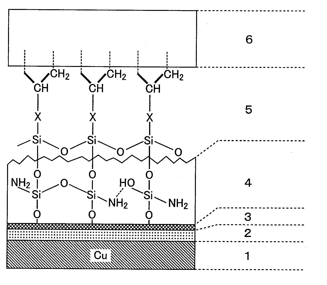
[0019]According to the present invention, the adhesion strength between the copper wiring having a smooth surface and the insulating layer comprising the low dielectric loss material can be increased, and the fine peeling between the insulating layer and the copper wiring can be prevented. Furthermore, according to the present invention, the dielectric loss and conductor loss of the multilayer wiring board can be both lowered, a high-frequency multilayer wiring board having high reliability such as solder heat resistance after moisture absorption and resistance to migration can be obtained.

Problems solved by technology

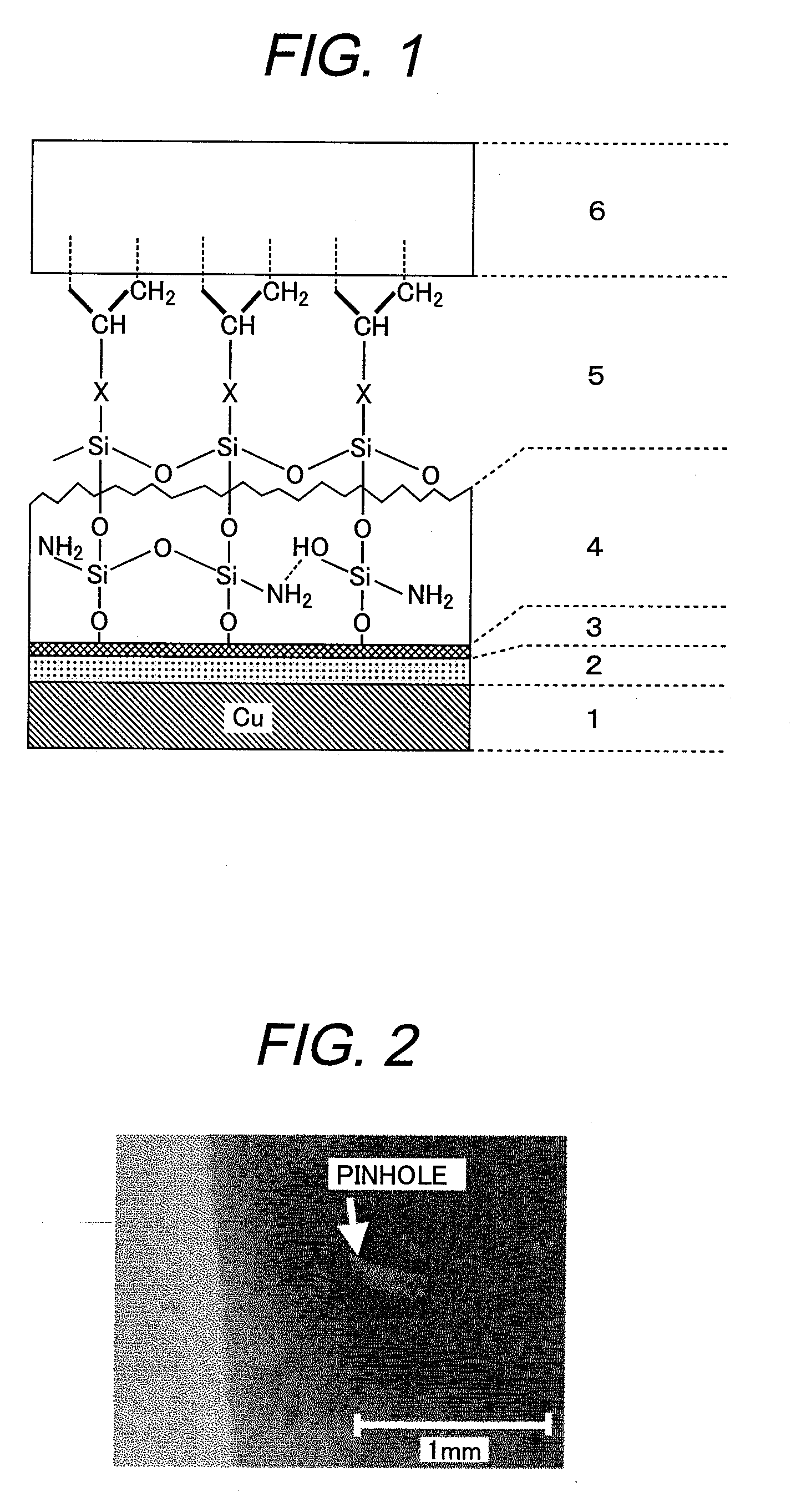
However, Although the adhesive strength for the low dielectric loss material is improved by providing the amino-silane coupling agent layer on the copper wiring, there was found the new problem that partial peeling occurs at the interface between the copper wiring and the low dielectric loss material under high-humidity / temperature conditions.

Method used


Image

  • Low dielectric loss wiring board, multilayer wiring board, copper foil and laminate
  • Low dielectric loss wiring board, multilayer wiring board, copper foil and laminate
  • Low dielectric loss wiring board, multilayer wiring board, copper foil and laminate

Examples


examples

[0070]Examples and Comparative Examples will be shown below to specifically describe the present invention.

[0071]First, reagents and evaluation methods are shown.

[0072](1) Synthesis of 1,2-bis(vinylphenyl)ethane (abbreviation: BVPE)

[0073]In a 500-ml three necked flask was placed 5.36 g (220 mmol) of granular magnesium (manufactured by Kanto Chemical Co., Inc.) for Grignard reaction. A dropping funnel, a nitrogen introducing pipe and a septum cap were attached to the flask. Under a stream of nitrogen, the entire system was dehydrated with heating while the magnesium grains were stirred with a stirrer. 300 ml of dried tetrahydrofuran was placed in a syringe, and was injected into the flask through the septum cap. After the solution was cooled to −5° C., 30.5 g (200 mmol) of vinylbenzyl chloride (manufactured by Tokyo Chemical Industry Co., Ltd.) was added dropwise over 4 hours using the dropping funnel. Stirring was continued at 0° C. for 20 hours after the completion of dropping.

[007...

examples 1 to 4

[0123]In Examples 1 to 4, copper foils with KBM-1043 applied as a vinyl-silane coupling agent on the amino-silane coupling agent layer of Comparative Example 1 were used to examine the effects of the multilayered silane coupling agent layers. The evaluation results of the adhesive strength for prepreg 1 are shown in Table 3. In Examples 1 to 4 using the multilayered silane coupling agent layers, the PCT resistance was improved. The values of their peel strength exhibited were higher than in the case where the amino-silane coupling agent layer or vinyl-silane coupling agent layer was singly used. The above results reasonably indicate that it is possible to obtain a copper-clad laminate, wiring board, and multilayer wiring board which are low both in dielectric loss and conductor loss, high in adhesive strength, and excellent in PCT resistance by providing the amino-silane coupling agent layer and the vinyl-silane coupling agent layer at the joining interface between the copper wiring...

examples 5 to 8

[0124]In Examples 5 to 8, copper foils with KBM-503 applied as the vinyl-silane coupling agent on the amino-silane coupling agent layer of Comparative Example 2 were used to examine the effects of the multilayered silane coupling agent layers. The evaluation results of the adhesive strength for prepreg 1 are shown in Table 4. In Examples 5 to 8 using the multilayered silane coupling agent layers, PCT resistance was improved. In addition, the values of the peel strength exhibited were high at the treatment concentration of the amino-silane coupling agent of 4 wt. % or lower and the treatment concentration of the vinyl-silane coupling agent of 1 wt. % or lower. The above results reasonably indicate that it is possible to obtain a copper-clad laminate, wiring board, and multilayer wiring board which are low in both dielectric loss and conductor loss, high in adhesive strength, and excellent in PCT resistance by providing the amino-silane coupling agent layer and vinyl-silane coupling a...


PUM

PropertyMeasurementUnit
surface roughnessaaaaaaaaaa
thicknessaaaaaaaaaa
thicknessaaaaaaaaaa

Abstract

A wiring board comprising a copper wiring, and an insulating layer which is a cured product of a resin composition containing a compound having a carbon-carbon unsaturated double bond as a cross-linking component,
    • the wiring board having a surface-treated layer formed on one or both sides of the copper wiring, and
    • the surface-treated layer having a metal layer (A) containing at least one metallic component selected from the group consisting of tin, zinc, nickel, chromium, cobalt and aluminium,
    • an oxide and/or hydroxide layer (B) of the metallic component on the metal layer (A),
    • an amino-silane coupling agent layer (C) having an amino group in its structure on the oxide and/or hydroxide layer (B), and
    • a vinyl-silane coupling agent layer (D) having a carbon-carbon unsaturated double bond on the amino-silane coupling agent layer (C).

Description

CLAIM OF PRIORITY[0001]The present application claims priority from Japanese patent application serial No. 2009-240975, filed on Oct. 20, 2009, the content of which is hereby incorporated by reference into this application.FIELD OF THE INVENTION[0002]The present invention relates to a wiring board, a multilayer wiring board, and a copper foil and a laminate for use in the same.BACKGROUND OF THE INVENTION[0003]Recently, electronic devices are increasingly reduced in size and weight, and high-density fine wiring is required for wiring boards used for such devices by means of multilayering and finer wiring. In order to achieve higher reliability of high-density fine wiring, enhanced adhesion of an insulating layer and copper wiring is required, and smoothing of adhesion interface from the perspective of improving accuracy of etching processing is required.[0004]Meanwhile, signal bands of information communication devices such as PHS and cellular phones, and CPU clock times of computers...

Claims


Application Information

Patent Timeline
Patent Type & Authority Applications(United States)
IPC IPC(8): H05K1/09B32B5/02B32B15/08
CPCH05K3/384H05K3/385H05K3/389H05K3/4611Y10T428/12438H05K2203/0315Y10T428/12472Y10T428/12444H05K2201/0355
Inventor AMOU, SATORUKAGIWADA, HIKARUHORI, DAI
Owner HITACHI LTD
Why Eureka
Try Eureka