Thin film transistor and manufacturing method thereof

a technology of thin film transistor and manufacturing method, which is applied in the direction of transistors, semiconductor devices, electrical devices, etc., can solve the problems of high manufacturing cost, inability to obtain sufficient switching characteristics, and low field effect mobility and small current, so as to achieve low current, high current, and high field effect mobility

Inactive Publication Date: 2011-06-23
SEMICON ENERGY LAB CO LTD
View PDF28 Cites 40 Cited by
  • Summary
  • Abstract
  • Description
  • Claims
  • Application Information

AI Technical Summary

Benefits of technology

[0024]As described above, a thin film transistor with low off current, high on current, and high field effect mobility can be manufactured with high productivity.

Problems solved by technology

A thin film transistor in which a channel is formed using an amorphous silicon layer has problems such as low field effect mobility and small on current.
On the other hand, a thin film transistor in which a channel is formed using a microcrystalline silicon layer has a problem in that, whereas the field effect mobility is higher than that of the thin film transistor in which a channel is formed using an amorphous silicon layer, off current is large, and thus sufficient switching characteristics cannot be obtained.
However, formation of the thin film transistor in which a channel formation region is formed using a polycrystalline silicon layer requires a crystallization step for a semiconductor layer and has a problem of higher manufacturing cost, as compared to the thin film transistor in which an amorphous silicon layer functions a channel formation region.
For example, a laser annealing technique involved in the process for forming a polycrystalline silicon layer has a problem in that large-screen liquid crystal panels cannot be produced efficiently because the laser beam irradiation area is small.

Method used


Image

  • Thin film transistor and manufacturing method thereof
  • Thin film transistor and manufacturing method thereof
  • Thin film transistor and manufacturing method thereof

Examples


embodiment 1

[0044]In this embodiment, a transistor according to one embodiment of the present invention will be described with reference to FIGS. 1A to 1D, FIG. 2, and FIGS. 3A to 3C. Note that an n-channel thin film transistor has higher carrier mobility than a p-channel thin film transistor. Further, it is preferable that all thin film transistors formed over the same substrate have the same polarity because the number of manufacturing steps can be reduced. In this embodiment, an n-channel thin film transistor will be described.

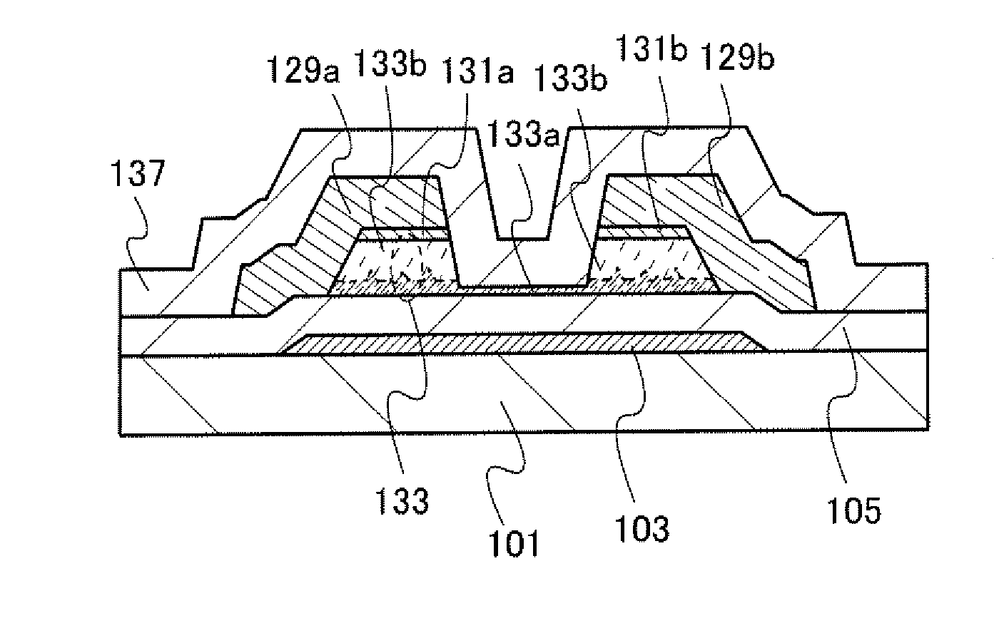
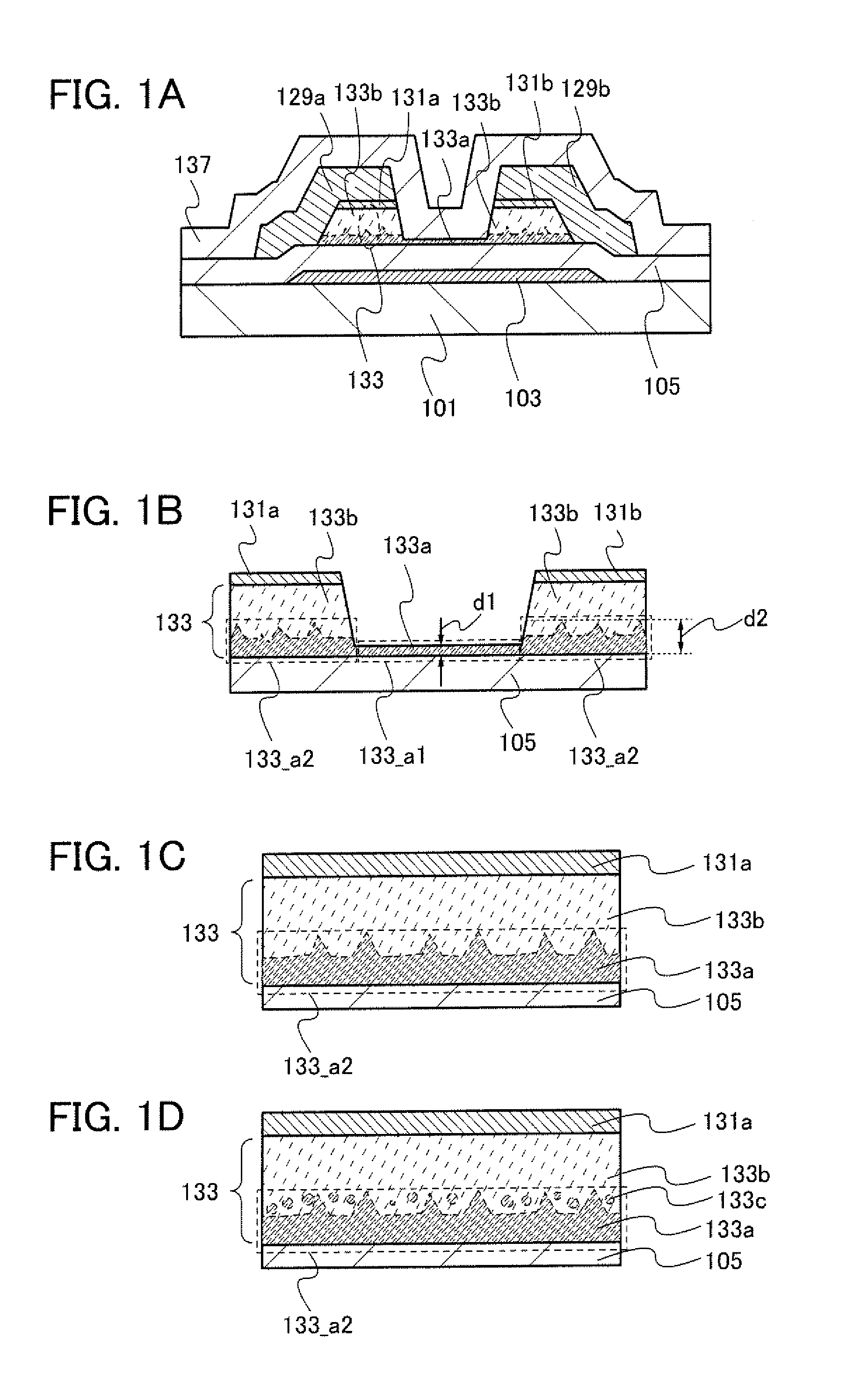
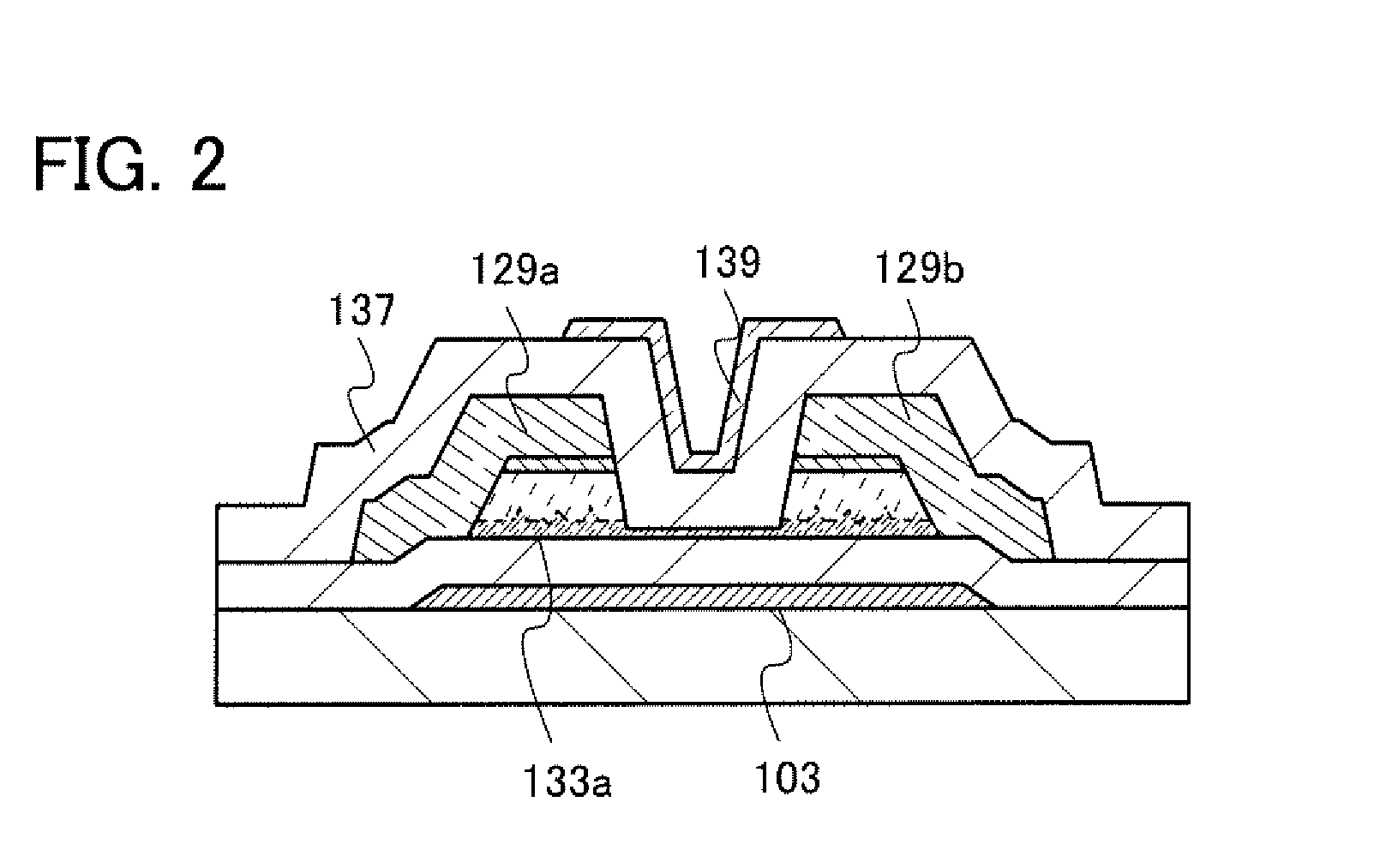
[0045]FIGS. 1A and 1B are cross-sectional views of a thin film transistor described in this embodiment.

[0046]The thin film transistor described in FIG. 1A includes, over a substrate 101, a gate electrode 103, a semiconductor layer 133, a gate insulating layer 105 provided between the gate electrode 103 and the semiconductor layer 133, impurity semiconductor layers 131a and 131b which are in contact with the semiconductor layer 133 and function as a source region and a ...

embodiment 2

[0087]In this embodiment, a thin film transistor having a structure different from that of Embodiment 1 will be described with reference to FIG. 4. In this embodiment, the shape of a semiconductor layer is different from that of Embodiment 1.

[0088]The thin film transistor illustrated in FIG. 4 includes, over the substrate 101, the gate electrode 103, a semiconductor layer 143, the gate insulating layer 105 provided between the gate electrode 103 and the semiconductor layer 143, the impurity semiconductor layers 131a and 131b which are in contact with the semiconductor layer 143 and function as a source region and a drain region, and the wirings 129a and 129b which are in contact with the impurity semiconductor layers 131a and 131b. The insulating layer 137 is formed so as to cover the semiconductor layer 143, the impurity semiconductor layers 131a and 131b, and the wirings 129a and 129b.

[0089]The semiconductor layer 143 includes a microcrystalline region 143a and a pair of amorphou...

embodiment 3

[0091]In this embodiment, a manufacturing method of the thin film transistors illustrated in FIGS. 1A to 1D and FIG. 2 will be described with reference to FIGS. 5A to 5C and FIGS. 6A to 6D. In this embodiment, a method for manufacturing an n-channel thin film transistor will be described.

[0092]As illustrated in FIG. 5A, the gate electrode 103 is formed over the substrate 101. Then, the gate insulating layer 105 and the microcrystalline semiconductor layer 107 are formed so as to cover the gate electrode 103.

[0093]As the substrate 101, the substrate 101 described in Embodiment 1 can be used as appropriate.

[0094]The gate electrode 103 is formed using any of the materials used for the gate electrode 103 described in Embodiment 1 as appropriate. The gate electrode 103 can be formed in such a manner that a conductive layer is formed over the substrate 101, using the above material by a sputtering method or a vacuum evaporation method, a mask is formed over the conductive layer by a photo...


PUM


Abstract

Disclosed is a thin film transistor including: a gate insulating layer covering a gate electrode; a microcrystalline semiconductor region over the gate insulating layer; a pair of amorphous semiconductor region over the microcrystalline semiconductor; a pair of impurity semiconductor layers over the amorphous semiconductor regions; and wirings over the impurity semiconductor layers. The microcrystalline semiconductor region has a surface having a projection and depression on the gate insulating layer side. The microcrystalline semiconductor region includes a first microcrystalline semiconductor region which is not covered with the amorphous regions and a second microcrystalline semiconductor region which is in contact with the amorphous semiconductor regions. A thickness d1 of the first microcrystalline semiconductor region is smaller than a thickness d2 of the second microcrystalline semiconductor region and d1 is greater than or equal to 30 nm.

Description

BACKGROUND OF THE INVENTION[0001]1. Field of the Invention[0002]The present invention relates to a thin film transistor and a method for manufacturing the thin film transistor, and a display device to which the thin film transistor is applied.[0003]2. Description of the Related Art[0004]As a kind of field-effect transistor, a thin film transistor in which a channel formation region is formed in a semiconductor layer formed over a substrate having an insulating surface is known. Techniques in which amorphous silicon, microcrystalline silicon, or polycrystalline silicon is used for a semiconductor layer used in the thin film transistor have been disclosed (see Patent Documents 1 to 5). A typical application of thin film transistors is a liquid crystal display television device, in which thin film transistors have been put to practical use as a switching transistor for each pixel that constitutes a display screen.REFERENCES[0005][Patent Document 1] Japanese Published Patent Application...

Claims


Application Information

Patent Timeline
Patent Type & Authority Applications(United States)
IPC IPC(8): H01L29/786H01L21/336
CPCH01L27/12H01L29/04H01L29/66765H01L27/124H01L29/78648H01L29/78678H01L29/78696H01L29/78618H01L27/1214H01L29/458
Inventor ISA, TOSHIYUKIHIROSE, ATSUSHI
Owner SEMICON ENERGY LAB CO LTD
Why Eureka
Try Eureka