Method for producing multilayer wiring substrate and multilayer wiring substrate

Inactive Publication Date: 2011-10-13
FUJIFILM CORP
View PDF5 Cites 30 Cited by
  • Summary
  • Abstract
  • Description
  • Claims
  • Application Information

AI Technical Summary

Benefits of technology

[0013]Namely, an object of the invention is to provide a method for producing a multilayer wiring substrate, which is suitable for forming a fine wiring in accordance with

Problems solved by technology

Therefore, owing to the irregularities of a substrate interface portion between the substrate and the obtained metal pattern, the wiring edge portion becomes rough, and there has been a problem in that the width of wiring lines cannot be made constant so that a wiring form according to designed values is less likely to obtain, or a portion that is connected to the adjacent wiring line may be produced or breaking of wiring lines may occur at the formation of a

Method used


Image

  • Method for producing multilayer wiring substrate and multilayer wiring substrate
  • Method for producing multilayer wiring substrate and multilayer wiring substrate
  • Method for producing multilayer wiring substrate and multilayer wiring substrate

Examples


example 1

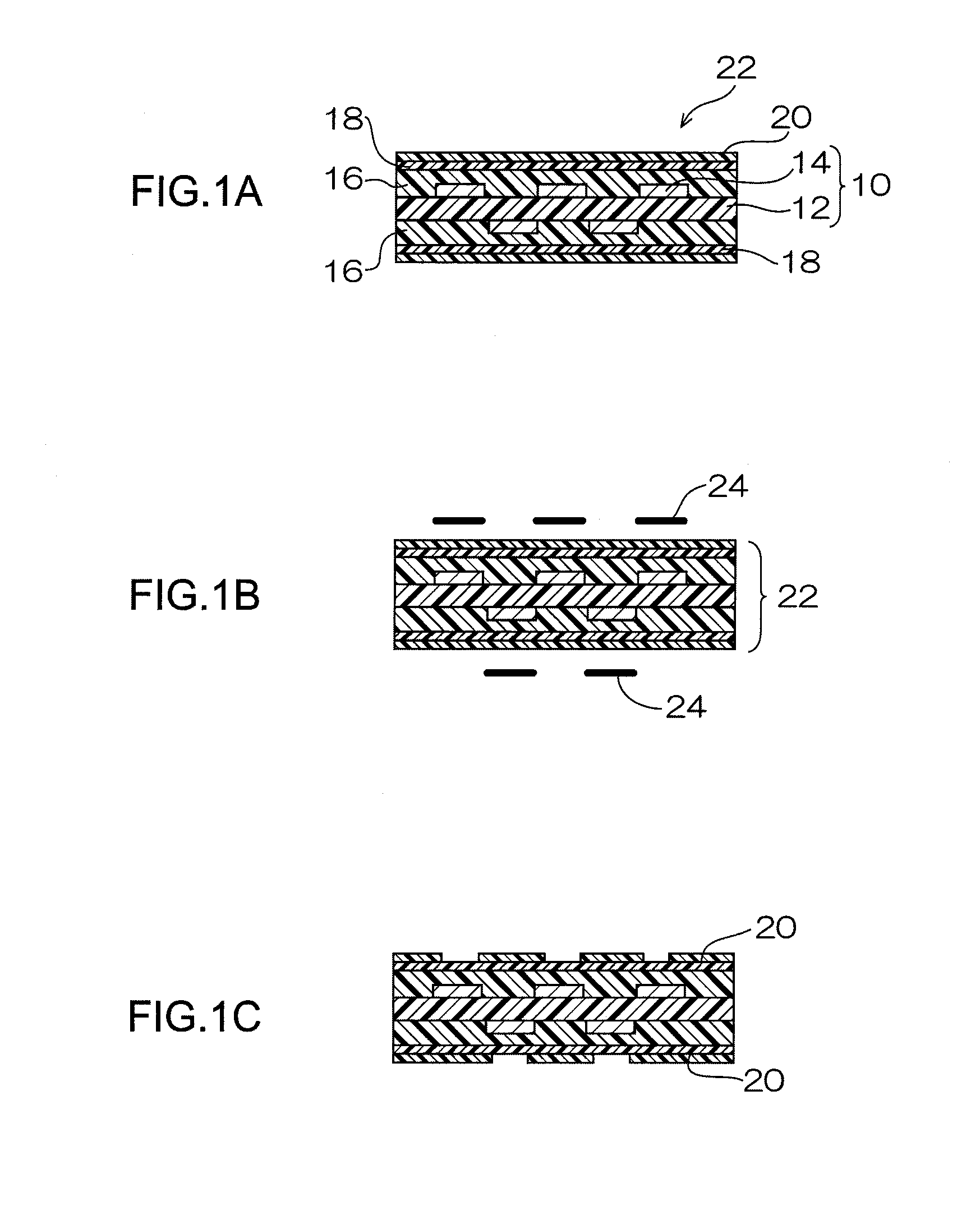
[0325]Preparation of Core Substrate

[0326]An insulating resin layer 16 was formed by attaching, as an electrically insulating layer, an epoxy-based insulating film (GX-13, trade name, manufactured by Ajinomoto Fine-Techno Co., Inc., thickness: 45 μm), to a glass epoxy substrate 12 on which a first wiring 14 was previously formed by a vacuum laminator, and heating and pressing under the conditions of temperature: 100 to 110° C. and pressure: 0.2 MPa.

[0327]Formation of Adhesion Auxiliary Layer

[0328]A coating liquid was prepared by mixing 11.8 parts by mass of JER 806 (bisphenol F-type epoxy resin, trade name, manufactured by Japan Epoxy Resins Co., Ltd.), 4.8 parts by mass of LA 7052 (PHENOLITE, trade name, curing agent, manufactured by DIC Corporation), 21.7 parts by mass of YP 50-35 EK (phenoxy resin, trade name, manufactured by Tohto Kasei Co., Ltd.), 61.6 parts by mass of cyclohexanone, and 0.1 part by mass of 2-ethyl-4-methyl imidazole (curing promotor), and then filtering the mix...

example 2

[0365]In order to produce a multilayer wiring substrate of an embodiment in which the inside of the via is filled with a metal by plating Preparation of a multilayer wiring substrate was conducted in a manner substantially similar to that in Example 1, except that the conditions of the above electroplating were changed to the following conditions.

[0366]Composition of Electroplating Bath

Copper (II) sulfate pentahydrate280gConcentrated sulfuric acid35gHydrochloric acid0.15mLCU-BRITE VF-II A (trade name, manufactured by 28.56mLEbara Udylite Co., Ltd.)CU-BRITE VF-II B (trade name, manufactured by1.46mLEbara Udylite Co., Ltd.)Distilled water1400g

[0367]Electroplating was conducted for 50 minutes under the condition of 2 A / dm2. The thickness of the obtained electric copper plated film was 20 μm.

[0368]When plating was conducted under the above conditions, the inside of the via was filled with copper.

[0369]Evaluation of Multilayer Wiring Substrate

[0370]The fine wiring thus formed was evaluat...

example 3

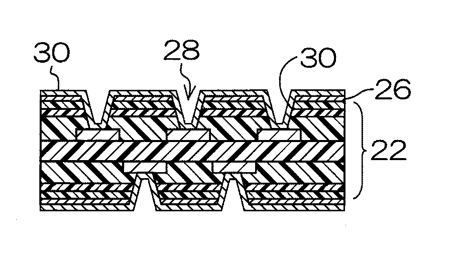
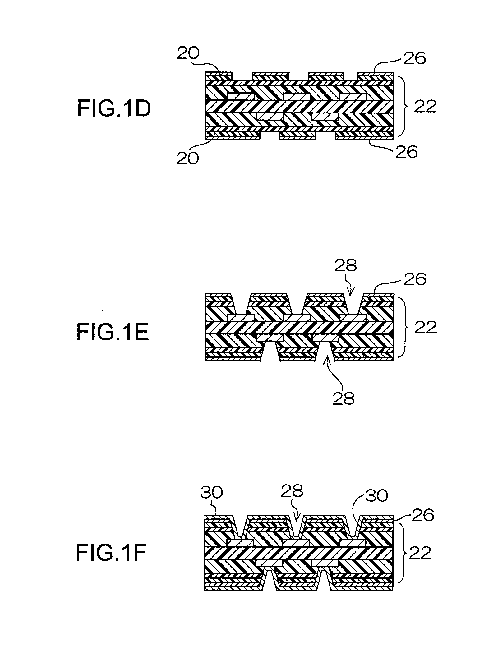
[0372]Preparation of a multilayer wiring substrate was conducted in a manner substantially similar to that in Example 1, except that, the conditions of the desmear treatment was changed in a manner such that the immersion in the etchant at a temperature of 80° C. for 10 minutes in Example 1 was changed to immersion in the etchant at a temperature of 75° C. for 5 minutes. Each Ra of the via-portion and the wiring portion was measured, and it was revealed that Ra of the via-portion was 0.39 μm, Ra of the second wiring portion was 0.08 μm, and the ratio of Ra of the second wiring portion to Ra of the inner face of the via-portion was 0.21. The formation of wiring could be conducted until the line / space reached 8 μm / 8 μm, and when the wiring form was observed, it was revealed that the shape of the edge portion of the wiring was a straight line. Furthermore, it was found that peeling off, floating, or the like did not occur at the wiring portion.


PUM

PropertyMeasurementUnit
Thicknessaaaaaaaaaa
Thicknessaaaaaaaaaa
Percent by volumeaaaaaaaaaa

Abstract

The present invention provides a method for producing a multilayer wiring substrate, including: forming a laminated body having an insulating resin layer and a polymer adhesive layer, on a surface of a first wiring substrate wherein the polymer adhesive layer contains a polymer precursor interacting with a plating catalyst or a precursor thereof, and a reactive group bonding with an adjacent layer on the first wiring substrate side; applying energy to a region outside of a via connection portion on the surface of the laminated body, to form a patterned polymer adhesive layer; applying a plating catalyst or a precursor thereof to the patterned polymer adhesive layer, and carrying out a first electroless plating, to form a second metal wiring on the surface of the patterned polymer adhesive layer; and forming a via by utilizing the patterned second metal wiring as a mask, and subsequently carrying out a desmear treatment.

Description

CROSS-REFERENCE TO RELATED APPLICATIONS[0001]This application is a continuation-in-part application of PCT application Ser. No. PCT / JP2009 / 068576, filed Oct. 29, 2009, which is based upon and claims the benefit of priority from prior Japanese Patent Application No. 2008-334602, filed Dec. 26, 2008. The entire contents of these applications are incorporated herein by reference in their entirety.BACKGROUND OF THE INVENTION[0002]1. Field of the invention[0003]The present invention relates to a method for producing a multilayer wiring substrate and a multilayer wiring substrate.[0004]2. Description of the Related Art[0005]Conventionally, a metal wiring substrate having wiring made of a metal pattern formed on a surface of an insulating substrate has been widely used for electronic components or semiconductor devices.[0006]Such a metal pattern material is produced mainly by a subtractive method. The subtractive method includes: forming a photosensitive layer that is sensitive to radiatio...

Claims


Application Information

Patent Timeline
IPC IPC(8): H05K1/03H05K3/10B05D1/38B05D5/12B05D3/00
CPCH05K3/0035H05K3/108H05K2203/0554H05K3/4661H05K2203/0525H05K3/387
Inventor TSURUMI, MITSUYUKI
Owner FUJIFILM CORP
Why Eureka
Try Eureka