Sputtering target, oxide semiconductor film and semiconductor device

a semiconductor film and target technology, applied in the direction of conductive materials, aluminum oxides/hydroxides, germanium dioxide, etc., can solve the problems of difficult to render the electron conductivity small, easy oxygen deficiency, and inability to show stable semiconductor properties of igzo semiconductors at high temperatures

Inactive Publication Date: 2011-12-29
IDEMITSU KOSAN CO LTD
View PDF1 Cites 39 Cited by
  • Summary
  • Abstract
  • Description
  • Claims
  • Application Information

AI Technical Summary

Benefits of technology

[0105]The sputtering target of the invention can be prepared by mixing and pulverizing material powders (raw material powders comprising indium oxide, at least one of gadolinium oxide, dysprosium oxide, holmium oxide, erbium oxide and ytterbium oxide to obtain a mixture, molding the mixture into a desired shape to obtain a shaped body, and sintering the shaped body.
[0106]In the above-mentioned method for producing a sputtering target of the invention, it is preferable to further add a material containing a positive divalent metal element and/or a metal element with an atomic valency of tetravalency or higher to the above-mentioned raw material powers.
[0107]As examples of the material containing a positive divalent metal element and/or a metal element with an atomic valency of positive tetravalency or higher, metals themselves or oxides of the above-mentioned positive divalent metal element and metal element with an atomic valency of positive tetravalency or higher can be used.
[0108]A

Problems solved by technology

Further, since most of the IGZO compositions show an amorphous phase, an IGZO semiconductor does not show stable semiconductor properties at high temperatures.
In the case of indium oxide alone, oxygen deficiency may tend to occur easily.
As a result, a large number of carrier electrons generate, which makes it difficult to render the electron conductivity small.
Therefore, when no transistor gate voltage is applied, a large amount of current tends to be flown between a source terminal and a drain terminal,

Method used


Image

  • Sputtering target, oxide semiconductor film and semiconductor device
  • Sputtering target, oxide semiconductor film and semiconductor device
  • Sputtering target, oxide semiconductor film and semiconductor device

Examples


preparation example 1

of a Field-Effect Thin Film Transistor

[0235]Next, the preparation example of a field-effect thin film transistor 1 using the above-mentioned crystalline oxide 21 will be explained with reference to the drawings.

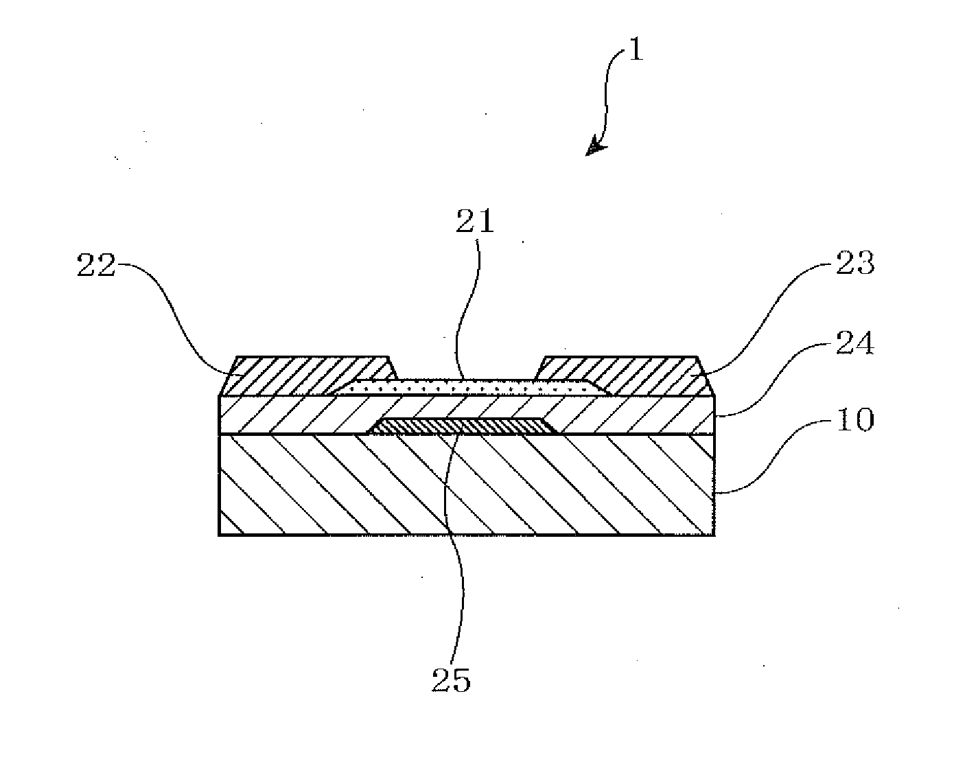
[0236]FIG. 6 is a schematic view of essential parts for explaining the method for producing a field-effect thin film transistor which is a semiconductor device according to one embodiment in the second aspect of the invention, in which (a) is a cross-sectional view showing the state in which a gate electrode is formed, (b) is a cross-sectional view showing the state in which a gate-insulating film is formed, and (c) is a cross-sectional view showing the state in which a crystalline oxide is formed.

[0237]As shown in FIG. 6(a), on a glass substrate 10, indium oxide containing tin oxide (10 wt %)(ITO) was formed into a film by a sputtering method with a substrate temperature being at 200° C. Subsequently, a photoresist was applied, and patterns of a gate electrode 25 and a wire ...

preparation example 2

of the Field-Effect Thin Film Transistor

[0257]FIG. 8 is a schematic cross-sectional view of a top-gate type field-effect thin film transistor which is a semiconductor device according to one embodiment in the second aspect of the invention.

[0258]In FIG. 8, a field-effect thin film transistor 1a of this preparation example is a top-gate thin film transistor, and is used in a TFT substrate or the like.

[0259]On the glass substrate 10, an IZO (registered trademark) with a large electroconductivity was stacked in a thickness of 40 nm by a sputtering film forming method. Then, a photoresist was applied, and by using a photomask, patterns of the source electrode 22, the drain electrode 23 and the wiring were exposed to light, followed by development with a developer. Then, by etching using a PAN-based etching solution (91.4 wt % of phosphoric acid, 3.3 wt % of nitric acid, and 5.3 wt % of acetic acid) of 45° C., the source electrode 22, the drain electrode 23 and the wiring were formed.

[02...

preparation example 3

of the Field-Effect Thin Film Transistor

[0264]The field-effect thin film transistor 1a of this preparation example is a top-gate thin film transistor as shown in FIG. 8.

[0265]At first, on the glass substrate 10, Au and IZO with a high electroconductivity (containing 10.7 wt % of zinc oxide) were respectively formed into a thickness of 50 nm by a sputtering film-forming method (Ar: 100%, total pressure: 0.3 Pa). Then, a photoresist was applied, and by using a photomask, patterns of the source electrode 22, the drain electrode 23 and the wiring were exposed to light, followed by development with a developer. Then, by etching with a PAN-based etching solution of 45° C. (91.4 wt % of phosphoric acid, 3.3 wt % of nitric acid and 5.3 wt % of acetic acid), the source electrode 22, the drain electrode 23 and the wiring were formed.

[0266]Next, on the glass substrate 10, an amorphous zinc oxide (5 at %) / indium oxide (95 at %) film to be used as the channel layer was formed in a thickness of 1...


PUM

PropertyMeasurementUnit
Fractionaaaaaaaaaa
Fractionaaaaaaaaaa
Fractionaaaaaaaaaa

Abstract

A sputtering target including an oxide sintered body, the oxide sintered body containing indium (In) and at least one element selected from gadolinium (Gd), dysprosium (Dy), holmium (Ho), erbium (Er) and ytterbium (Yb), and the oxide sintered body substantially being of a bixbyite structure.

Description

TECHNICAL FIELD[0001]The invention relates to a sputtering target and an oxide semiconductor film. The invention relates to a semiconductor device, in particular, to a semiconductor device using as a semiconductor crystalline indium oxide having a prescribed electron carrier concentration.BACKGROUND ART[0002]An oxide semiconductor film composed of a metal composite oxide has a high degree of mobility and excellent visible light transmission, and is used as a switching element, a driving circuit element or the like for a liquid crystal display, a thin film electroluminescence display, an electrophoresis display, a moving powder display, etc.[0003]As the oxide semiconductor film composed of such a metal composite oxide, a zinc oxide-based crystalline thin film (Patent Document 1) has attracted attention. However, zinc oxide has a defect that it lacks stability, and hence, a very few of them were put into practical use.[0004]Non-patent Document 1 discloses a thin film transistor using ...

Claims


Application Information

Patent Timeline
IPC IPC(8): C01F17/00C01G15/00C01F5/00C23C14/34C01G51/04C01B35/00C01F7/02H01B1/08C01G53/04
CPCC23C14/086H01L29/66969H01L29/7869C04B35/01C04B2235/3201C04B2235/3203C04B2235/3206C04B2235/3217C04B2235/3224C04B2235/3225C04B2235/3229C04B2235/3232C04B2235/3244C04B2235/3251C04B2235/3275C04B2235/3279C04B2235/3281C04B2235/3284C04B2235/3286C04B2235/3287C04B2235/3409C04B2235/72C04B2235/77C04B2235/81C23C14/3414H01L29/26H01L29/66742
Inventor INOUE, KAZUYOSHIYANO, KOKIKASAMI, MASASHI
Owner IDEMITSU KOSAN CO LTD
Why Eureka
Try Eureka