Semiconductor device and manufacturing method thereof

a technology of semiconductor devices and semiconductors, applied in semiconductor devices, electric lighting sources, electric light sources, etc., can solve the problems of high process temperature, low mass productivity of semiconductor devices using compound semiconductors such as silicon carbide or gallium nitride, and the inability to meet the allowable temperature limit, etc., to achieve high process temperature, low power consumption, and high reliability

Active Publication Date: 2012-06-14
SEMICON ENERGY LAB CO LTD
View PDF2 Cites 46 Cited by
  • Summary
  • Abstract
  • Description
  • Claims
  • Application Information

AI Technical Summary

Benefits of technology

[0006]As for a transistor included in a semiconductor device, it is preferable to reduce the variation of the threshold voltage caused by time degradation and to reduce the off-state current. With the transistor the variation of the threshold voltage caused by time degradation of which is small, reliability of a semiconductor device can be increased. With a transistor the off-state current of which is low, power consumption of a semiconductor device can be suppressed.
[0007]It is an object of the present invention to provide a method for manufacturing a highly reliable semiconductor device. It is another object of the present invention to provide a method for manufacturing a semiconductor device with low power consumption. It is another object of the present invention to provide a highly reliable semiconductor device. It is another object of the present invention to provide a semiconductor device with low power consumption.
[0008]In a semiconductor device with high withstand voltage for controlling large current, a so-called power device, silicon has been used mainly as a semiconductor material. However, it is said that the physical characteristics of a semiconductor element using silicon reach the theoretical value limit, and a novel semiconductor material with which the characteristics can be improved has been demanded in order to realize a power device that has high withstand voltage and can control large current. As the semiconductor material that may improve the characteristics such as high withstand voltage, high conversion efficiency, or high-speed switching, for example, a compound semiconductor such as silicon carbide or gallium nitride can be given. The bandgap of silicon carbide and the bandgap of gallium nitride are 3.26 eV and 3.39 eV, respectively, which are about three times as large as that of silicon; it is known that such a compound semiconductor is advantageous for improving the withstand voltage, reducing the power loss of a semiconductor device, and the like.

Problems solved by technology

On the other hand, the compound semiconductor such as silicon carbide or gallium nitride has a problem of high process temperature.
The process temperature of silicon carbide is about 1500° C. and the process temperature of gallium nitride is about 1100° C., which does not allow film deposition on a glass substrate whose allowable temperature limit is low.
Therefore, an inexpensive glass substrate cannot be used, and further, the compound semiconductor cannot be applied when the size of a substrate is increased, so that the mass productivity of semiconductor devices using the compound semiconductor such as silicon carbide or gallium nitride is low, which disturbs practical application.

Method used


Image

  • Semiconductor device and manufacturing method thereof
  • Semiconductor device and manufacturing method thereof
  • Semiconductor device and manufacturing method thereof

Examples


embodiment 1

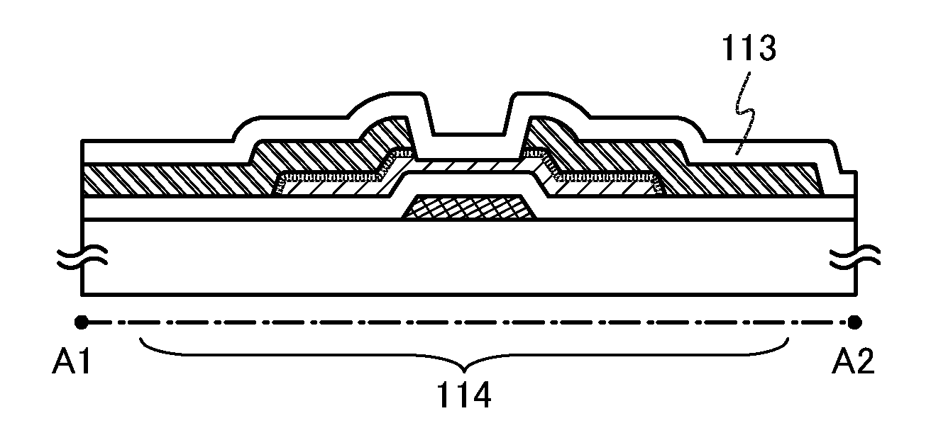
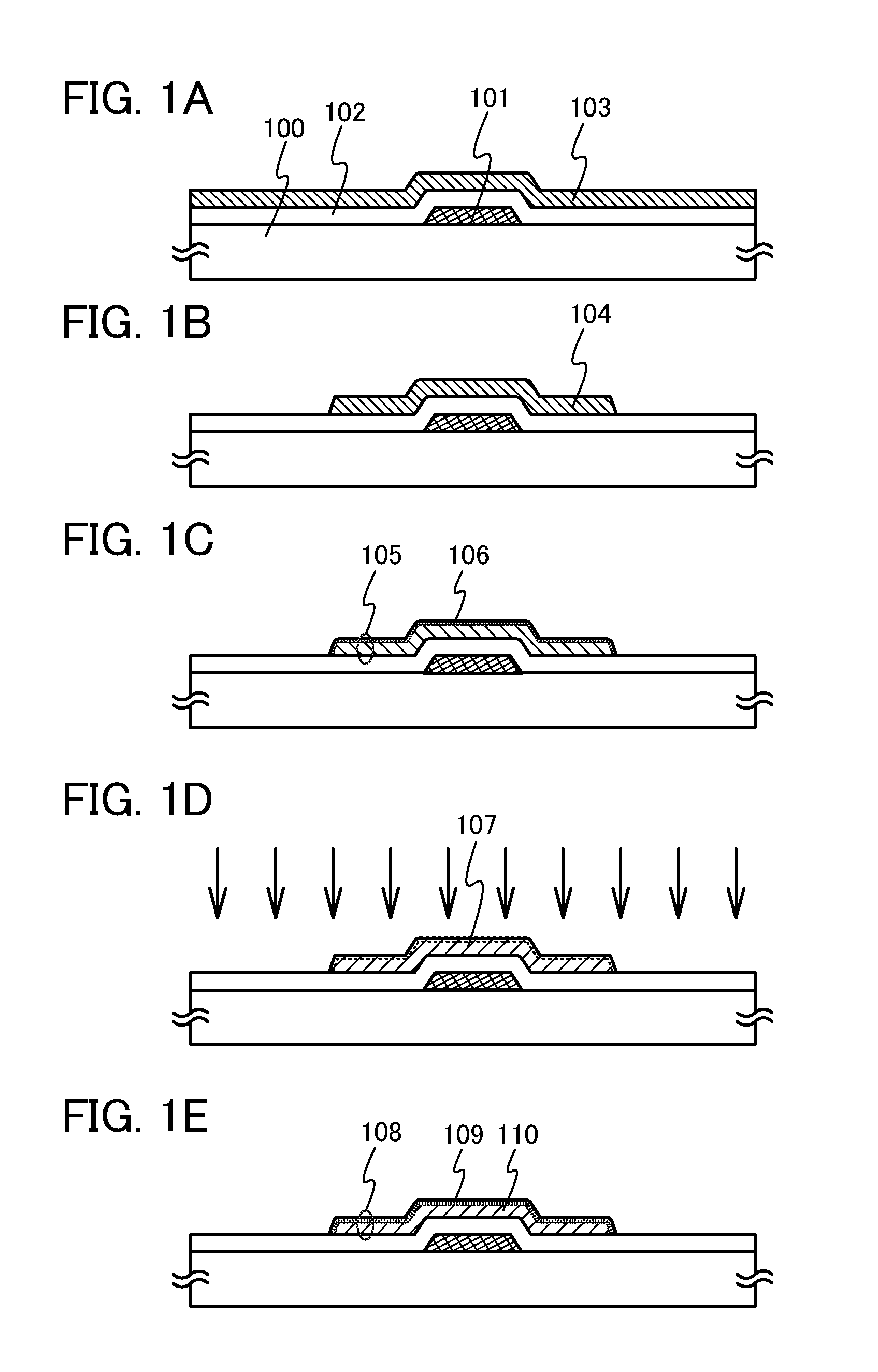
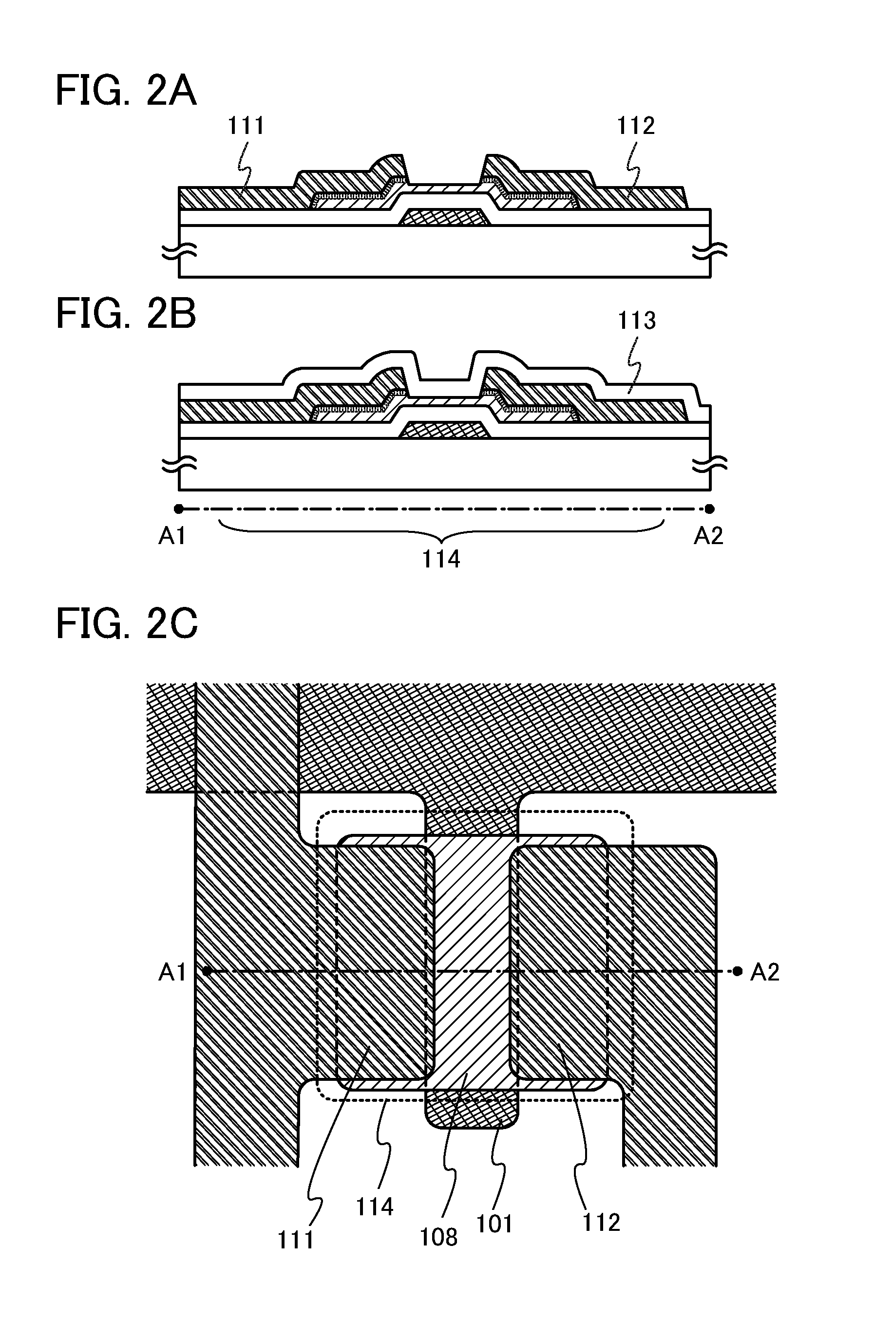
[0056]A bottom-gate transistor having a channel-etched structure is taken as an example, and a structure of the transistor included in a semiconductor device according to one embodiment of the present invention and a manufacturing method thereof will be described.

[0057]As shown in FIG. 1A, a gate electrode 101 is formed over a substrate 100.

[0058]Although there is no particular limitation on a substrate that can be used as the substrate 100 having an insulating surface, it is necessary that the substrate has heat resistance high enough to withstand at least heat treatment to be performed later. For example, a glass substrate manufactured by a fusion method or a float method can be used. When the temperature of the heat treatment performed later is high, it is preferable to use a substrate having a strain point of 730° C. or higher as the glass substrate. For the glass substrate, a glass material such as aluminosilicate glass, aluminoborosilicate glass, or barium borosilicate glass i...

embodiment 2

[0167]In Embodiment 2, a structure and a manufacturing method of a transistor for a power device capable of higher voltage or higher current control will be described. Embodiment 1 can be applied to the same portions as Embodiment 1 or portions having functions similar to those of Embodiment 1, and therefore, description thereof is not omitted.

[0168]As shown in FIG. 5A, an insulating film 201 which serves as a base film is formed over a substrate 200, and then, a first electrode 202 is formed.

[0169]The description on the substrate 100 described in Embodiment 1 can be referred to for a substrate to be used as the substrate 200. The description on the base film described in Embodiment 1 can be referred to for a material, the structure, and the thickness of the insulating film 201.

[0170]The first electrode 202 is formed using a metal element selected from aluminum, chromium, copper, tantalum, titanium, molybdenum, tungsten, or yttrium; an alloy containing any of these metal elements as...

embodiment 3

[0267]In Embodiment 3, a structure and a method for manufacturing a semiconductor device will be described using a bottom-gate transistor having a channel protective structure as an example. Embodiment 1 can be applied to the same portions as Embodiment 1 or portions having functions similar to those of Embodiment 1, and therefore, description thereof is not omitted.

[0268]The state shown in FIG. 1E described in Embodiment 1 is obtained through the process up to and including the second heat treatment in a similar manner. Next, as shown in FIG. 8A, a channel protective film 130 is formed over the oxide semiconductor film 108 so as to overlap with a region of the oxide semiconductor film 108, which overlaps with the gate electrode 101, that is, so as to overlap with a channel formation region. The channel protective film 130 can prevent the portion of the oxide semiconductor film 108, which serves as the channel formation region, from being damaged in a later step (for example, reduct...


PUM


Abstract

A semiconductor device for high power application in which a novel semiconductor material having high mass productivity is provided. An oxide semiconductor film is formed, and then, first heat treatment is performed on the exposed oxide semiconductor film in order to reduce impurities such as moisture or hydrogen in the oxide semiconductor film. Next, in order to further reduce impurities such as moisture or hydrogen in the oxide semiconductor film, oxygen is added to the oxide semiconductor film by an ion implantation method, an ion doping method, or the like, and after that, second heat treatment is performed on the exposed oxide semiconductor film.

Description

TECHNICAL FIELD[0001]The present invention relates to a semiconductor device using an oxide semiconductor and a manufacturing method thereof.BACKGROUND ART[0002]A transistor using a semiconductor film formed over an insulating surface is an essential semiconductor element for a semiconductor device. Since the manufacturing of transistors has a limitation on the allowable temperature limit of a substrate, a transistor using, as an active layer, amorphous silicon which can be formed at a relatively low temperature, polysilicon which can be obtained by crystallization using laser light or a catalytic element, or the like has been mainly used as a transistor for the semiconductor display device.[0003]In recent years, a metal oxide having semiconductor characteristics which is referred to as an oxide semiconductor has attracted attention as a novel semiconductor material which has both high mobility, which is a characteristic of polysilicon, and uniform element characteristics, which is ...

Claims


Application Information

Patent Timeline
Patent Type & Authority Applications(United States)
IPC IPC(8): H01L21/36H05B44/00
CPCH01L21/28176H01L21/324H01L29/04H01L29/66742H01L29/78603H01L29/66969H01L29/78618H01L29/78642H01L29/78648H01L29/7869H01L29/78696H01L29/78606H01L21/465H01L21/477H01L21/02554H01L21/02565H01L29/045
Inventor YAMAZAKI, SHUNPEISAKATA, JUNICHIROOHARA, HIROKI
Owner SEMICON ENERGY LAB CO LTD
Why Eureka
Try Eureka