Mask blank, transfer mask, method of manufacturing a transfer mask, and method of manufacturing a semiconductor device

Active Publication Date: 2012-06-21
HOYA CORP
View PDF1 Cites 13 Cited by
  • Summary
  • Abstract
  • Description
  • Claims
  • Application Information

AI Technical Summary

Benefits of technology

[0089]According to this invention, it is possible to provide a mask blank which enables a defect correction technique using charged particle irradiation to be suitably applied to a transfer mask manufactured from the mask blank and which can make sma

Problems solved by technology

As a result, it has been found that the following problems may occur depending on the relationship between the film compositions in the upper and lower layers of the laminated structure.
However, in the case of nitrided, oxidi

Method used


Image

  • Mask blank, transfer mask, method of manufacturing a transfer mask, and method of manufacturing a semiconductor device
  • Mask blank, transfer mask, method of manufacturing a transfer mask, and method of manufacturing a semiconductor device
  • Mask blank, transfer mask, method of manufacturing a transfer mask, and method of manufacturing a semiconductor device

Examples


example 1

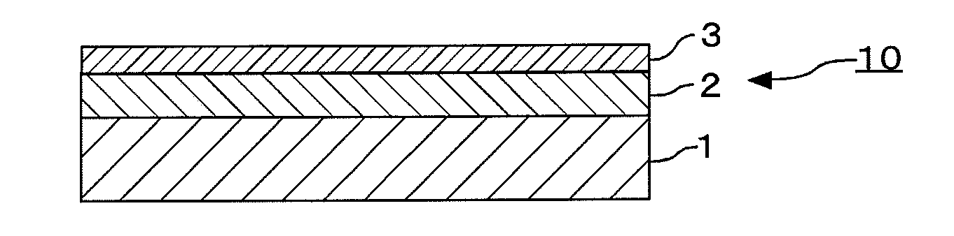
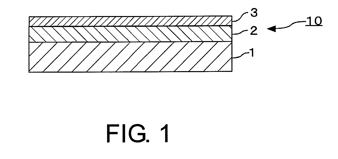
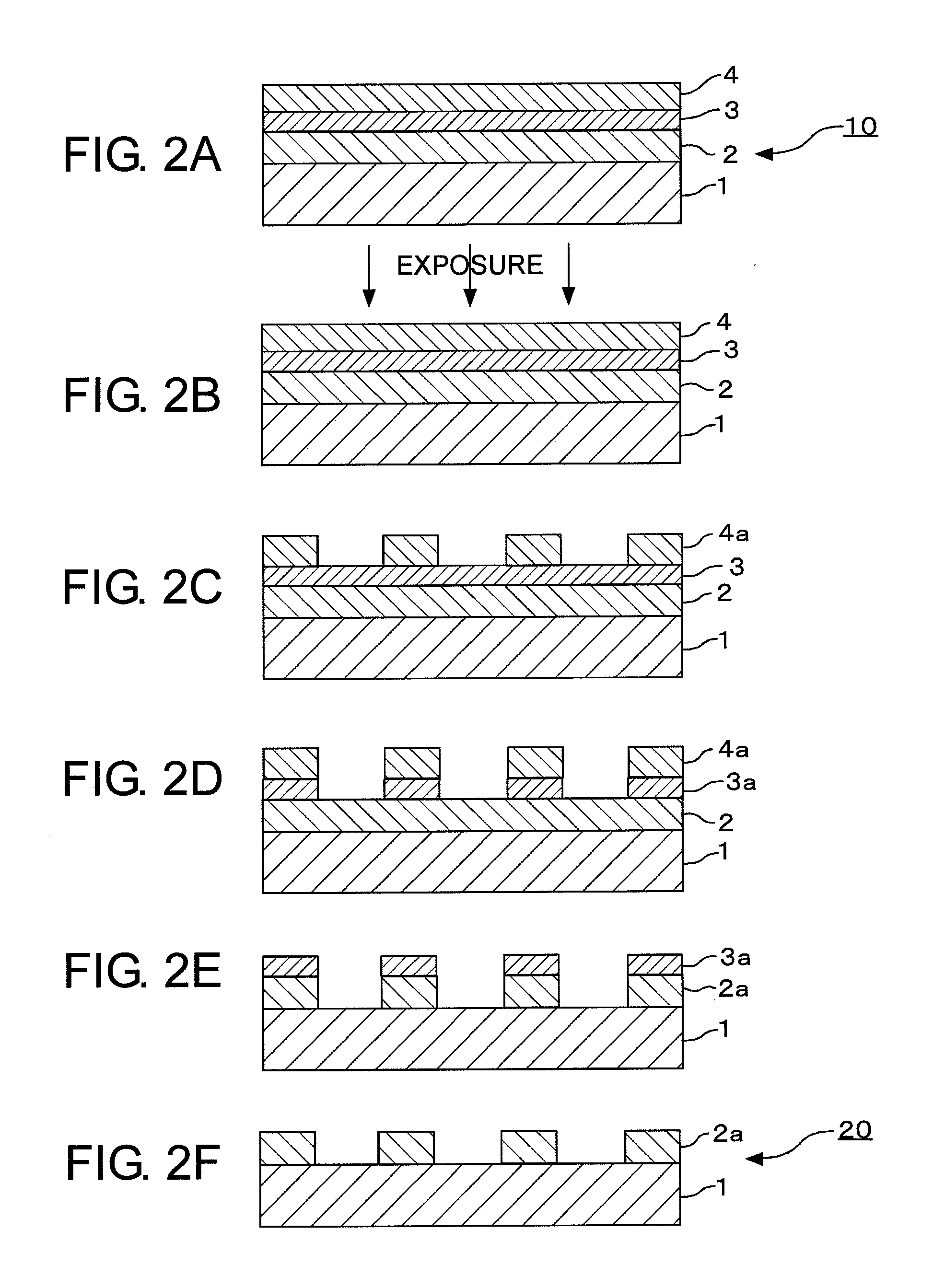
[0135]In a single-wafer sputtering apparatus, using a mixed target of molybdenum (Mo) and silicon (Si) (at % ratio Mo:Si=13:87) as a sputtering target, reactive sputtering (DC sputtering) was carried out in a mixed gas atmosphere of argon and nitrogen, thereby forming a MoSiN film (lower layer (light-shielding layer)) to a thickness of 47 nm on a transparent substrate 1 made of synthetic quartz glass. Then, using a Mo / Si target (at % ratio Mo:Si=13:87), reactive sputtering (DC sputtering) was carried out in a mixed gas atmosphere of argon and nitrogen, thereby forming a MoSiN film (upper layer (front-surface antireflection layer)) to a thickness of 4 nm on the lower MoSiN film. In this manner, a light-shielding film 2 (total thickness: 51 nm) for ArF excimer laser light (wavelength: 193 nm) was formed.

[0136]Then, the substrate 1 with the light-shielding film 2 was heat-treated (annealed) at 450° C. for 30 minutes, thereby reducing the film stress of the light-shielding film 2. A sub...

example 2

[0137]In a single-wafer sputtering apparatus, using a mixed target of molybdenum (Mo) and silicon (Si) (at % ratio Mo:Si=13:87) as a sputtering target, reactive sputtering (DC sputtering) was carried out in a mixed gas atmosphere of argon and nitrogen, thereby forming a MoSiN film (lower layer (light-shielding layer)) to a thickness of 46 nm on a transparent substrate 1 made of synthetic quartz glass. Then, using a Mo / Si target (at % ratio Mo:Si=13:87), reactive sputtering (DC sputtering) was carried out in a mixed gas atmosphere of argon and nitrogen, thereby forming a MoSiN film (upper layer (front-surface antireflection layer)) to a thickness of 3 nm on the lower MoSiN film. In this manner, a light-shielding film 2 (total thickness: 49 nm) for ArF excimer laser light (wavelength: 193 nm) was formed.

[0138]Then, the substrate 1 with the light-shielding film 2 was heat-treated (annealed) at 450° C. for 30 minutes, thereby reducing the film stress of the light-shielding film 2. A sub...

reference example 1

[0139]In a single-wafer sputtering apparatus, using a mixed target of molybdenum (Mo) and silicon (Si) (at % ratio Mo:Si=13:87) as a sputtering target, reactive sputtering (DC sputtering) was carried out in a mixed gas atmosphere of argon and nitrogen, thereby forming a MoSiN film (lower layer (light-shielding layer)) to a thickness of 47 nm on a transparent substrate 1 made of synthetic quartz glass. Then, using a Mo / Si target (at % ratio Mo:Si=13:87), reactive sputtering (DC sputtering) was carried out in a mixed gas atmosphere of argon and nitrogen, thereby forming a MoSiN film (upper layer (front-surface antireflection layer)) to a thickness of 13 nm on the lower MoSiN film. In this manner, a light-shielding film 2 (total thickness: 60 nm) for ArF excimer laser light (wavelength: 193 nm) was formed.

[0140]Then, the substrate 1 with the light-shielding film 2 was heat-treated (annealed) at 450° C. for 30 minutes, thereby reducing the film stress of the light-shielding film 2. A su...


PUM


Abstract

A mask blank for use in the manufacture of a transfer mask adapted to be applied with ArF excimer laser exposure light is disclosed. The mask blank has, on a transparent substrate, a light-shielding film for forming a transfer pattern. The light-shielding film has an at least two-layer structure including a lower layer and an upper layer from the transparent substrate side. The lower layer is made of a material composed of a transition metal, silicon, and nitrogen and having a nitrogen content of 21 at % or more and a refractive index n of 1.9 or less. The upper layer is made of a material composed of a transition metal, silicon, and nitrogen and having a refractive index n of 2.1 or less. A surface layer of the upper layer contains oxygen and has a nitrogen content of 14 at % or more.

Description

[0001]This application is based upon and claims the benefit of priority from Japanese Patent Application No. 2010-281333, filed on Dec. 17, 2010, the disclosure of which is incorporated herein in its entirety by reference.TECHNICAL FIELD[0002]This invention relates to a mask blank, a transfer mask, a method of manufacturing a transfer mask, and a method of manufacturing a semiconductor device. In particular, this invention relates to a mask blank which enables a defect correction technique using charged particle irradiation to be suitably applied to a transfer mask manufactured from the mask blank and which can make small a bias for the transfer mask due to an electromagnetic field (EMF) effect, and further relates to such a transfer mask, a method of manufacturing such a transfer mask, and a method of manufacturing a semiconductor device using such a transfer mask.BACKGROUND ART[0003]Generally, fine pattern formation is carried out by the photolithography in the manufacture of a se...

Claims


Application Information

Patent Timeline
IPC IPC(8): G03F7/00G03F1/72B32B7/02G03F1/00
CPCG03F1/58G03F1/00Y10T428/24942G03F1/74G03F7/2006G03F1/50G03F1/38G03F1/46H01L21/0274H01L21/0337
Inventor KOMINATO, ATSUSHIHASHIMOTO, MASAHIROIWASHITA, HIROYUKI
Owner HOYA CORP
Why Eureka
Try Eureka