Method for Fabricating Organic Devices

a technology of organic devices and manufacturing methods, applied in the direction of solid-state device manufacturing, electric devices, semiconductor/solid-state device manufacturing, etc., can solve the problems of unstable silane layer on gold (oxide), less uniform surface, and non-uniform thickness of metal contacts, etc., to achieve good morphology, good mobility, and good performance

Inactive Publication Date: 2012-08-23
INTERUNIVERSITAIR MICRO ELECTRONICS CENT (IMEC VZW) +1
View PDF0 Cites 5 Cited by
  • Summary
  • Abstract
  • Description
  • Claims
  • Application Information

AI Technical Summary

Benefits of technology

[0092]In a method according to the first aspect, after providing on a substrate a dielectric layer and after providing bottom contact structures, for example by means of a lift-off technique or by any other suitable technique known by a person skilled in the art, a temporary protection layer may be provided on the bottom contact structures. Providing the temporary protection layer can for example be performed during the preparation of the bottom contact structures, for example using a lift-off process. Alternatively, providing the temporary protection layer can be performed in a separate step, after forming the bottom contact structures. After providing the bottom contact structures, an UV-ozone cleaning step may be performed (either before or after providing the temporary protection layer). Next a first surface modification layer, e.g. a silane layer, an organic phosphonic acid layer or a carboxylic acid layer, may be provided at least on the dielectric layer surface. Then the temporary protection layer may be removed by a chemical treatment that does not deteriorate the first surface modification layer, e.g. silane layer. In a next step a second surface modification layer, preferably a SAM, e.g. comprising thiols, organic disulfides, substituted thioureas, isothiocyanates, thiophenes, imidazole-2-thiones, selenols, organic diselenides, nitriles, isonitriles, or thioacetates, may be provided selectively on the bottom contacts. After that, an organic semiconductor layer, e.g. a pentacene layer, with a good morphology and a good mobility can be formed. In preferred embodiments the first temporary protection layer and / or the second temporary protection layer may be selected such that they lead to a hydrophobic surface.
[0093]It is an advantage of a method according to embodiments of the present invention that the second surface modification layer (e.g. a self-assembled monolayer, a dopant or a compound (deliberately) made by partial reaction of the bottom contact metal with an electron acceptor) is provided after providing the first surface modification layer (e.g. silane), such that degradation of the second surface modification layer (e.g. a self-assembled monolayer, a dopant or a compound deliberately made by partial reaction of the bottom contact metal with an electron acceptor) by providing the first surface modification layer (e.g. silane) (as in prior art methods) can be avoided.
[0094]It is an advantage of a method according to the present invention that the formation of a metal oxide, e.g. gold oxide, on the bottom contact structure, e.g. gold bottom contact structure, can be avoided. In prior art methods such a metal oxide, e.g. gold oxide, may be formed during UV ozone cleaning after formation of the bottom contacts. Avoiding the formation of a metal oxide on the bottom contact structure, e.g. by providing a temporary protection layer as described in embodiments of the present invention, enables the use of lift-off techniques for forming the bottom contacts (without contamination or deterioration by e.g. a metal oxide layer), and thus the realisation of small channel lengths, leading to organic transistors with good performance. A method of the present invention can also be used for fabricating transistors with large channel lengths, e.g. channel lengths up to several hundreds of micrometers.
[0095]It is an advantage of a method according to embodiments of the present invention that bottom-contact pentacene transistors comprising contacts based on other materials than gold, e.g. materials that would not withstand the UV-ozone cleaning, e.g. bottom contacts based on Ag, Cu, Ni, . . . , can be fabricated. It is an advantage that the price of these materials is lower than the price of gold, such that cheaper organic circuits could be made. The bottom contacts can comprise a single metal (eventually with an adhesion layer underneath) or the bottom contacts can comprise two or more metals, e.g. a stack of layers comprising different metals or a metal alloy.

Problems solved by technology

Therefore, when reversing the sequence of surface treatment steps (i.e. first performing a silane treatment and afterwards performing a thiol treatment), the silanes may bond to the (unstable) gold oxide, and thus the silane layer on the gold (oxide) would also be unstable.
In case of solution phase silanization not only a monolayer, but sometimes also additional silane may be present on the substrate, leading to a less uniform surface.
Using shadow mask techniques for forming the metal contacts may lead to a non-uniform thickness of the metal contacts (i.e. with ‘spikes’ at the edges).
When using shadow mask techniques the obtainable channel length is relatively large (typically several tens of micrometers) and thus the frequency of the corresponding circuits is limited.
However, lift-off techniques require photoresists, developers, solvents, .

Method used


Image

  • Method for Fabricating Organic Devices
  • Method for Fabricating Organic Devices
  • Method for Fabricating Organic Devices

Examples


example 1

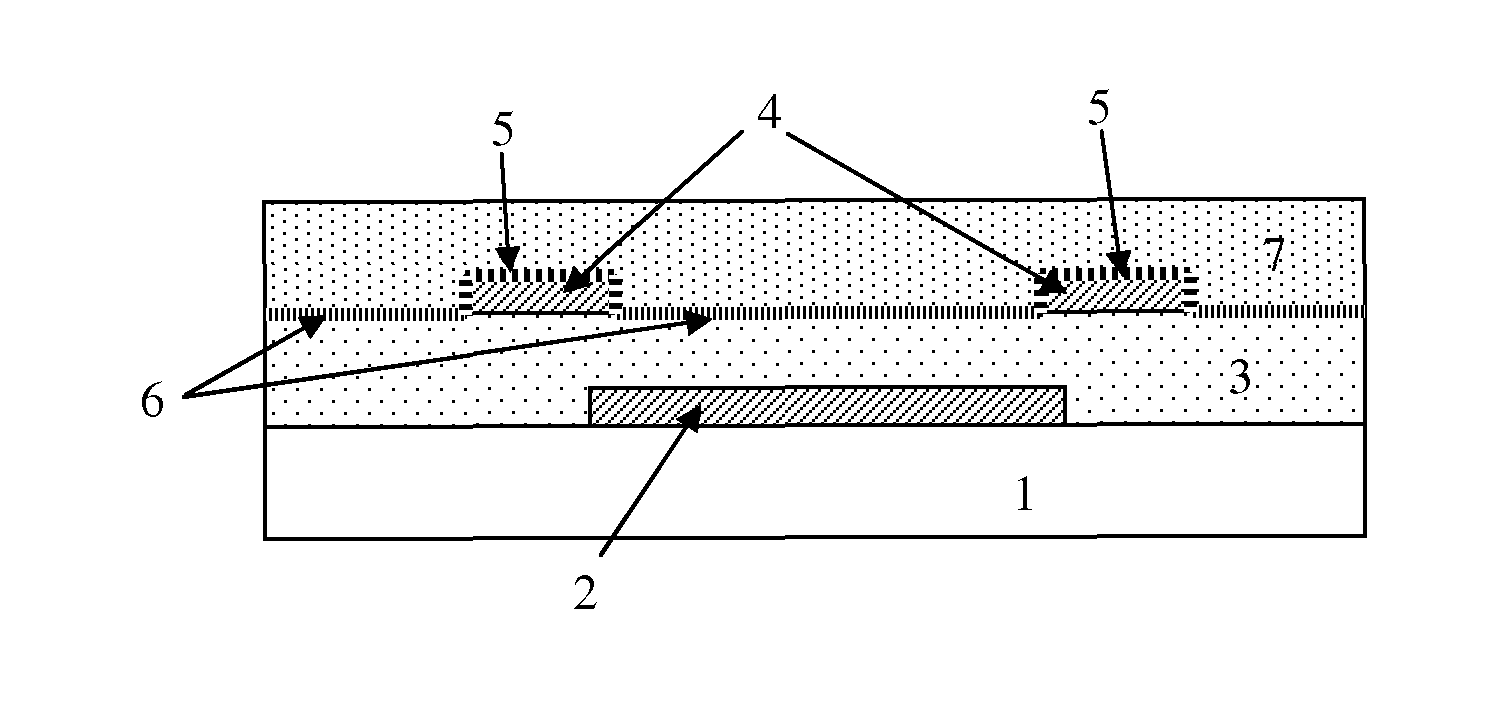
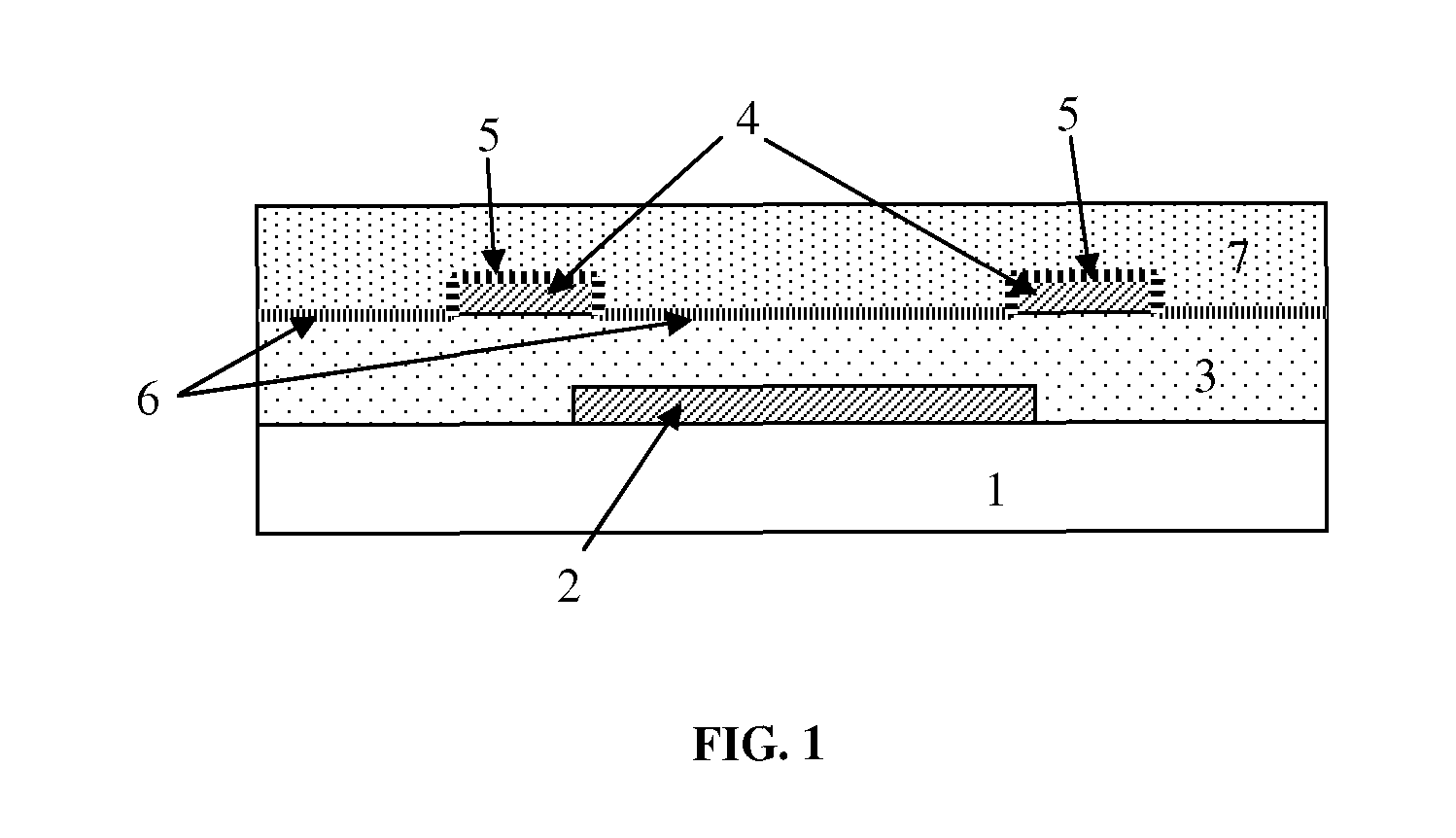
Au Bottom Contact Transistors

[0144]Au bottom-contact organic transistors were prepared by a fabrication process using lift-off for the formation of the bottom metal contacts. In the experiments, silicon substrates comprising a common aluminum gate and a 140 nm thick dielectric layer (silicon dioxide) were used. After cleaning of the substrate a patterned photoresist layer was provided, followed by a metallization step comprising sputtering of a 20 nm thick gold layer and a 5 nm thick aluminum layer. Next a lift-off step was performed in an ultrasonic bath with acetone. In the transistor structure, the 20 nm thick gold layer forms the source and the drain of the transistor. The 5 nm aluminum layer acts as a temporary protection layer in accordance with an embodiment of the present invention.

[0145]After wet cleaning and UV-ozone cleaning (15 minutes) of the samples, a silane treatment was performed wherein PETS (phenylethyltrichlorosilane) was provided from the vapor phase at a temper...

example 2

Ag Bottom Contact Transistors

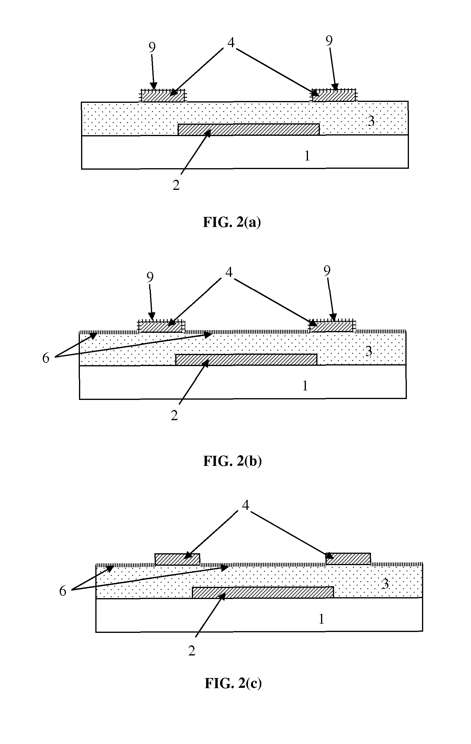
[0147]Experiments were performed wherein Ag bottom contact transistors were fabricated according to a method according to an embodiment of the present invention. A metallization step was performed comprising providing a stack of a 15 nm thick Au layer (acting as an adhesion layer) and a 20 nm thick Ag layer (acting as bottom contact metal from which also an “injection layer” can be made by partial chemical reaction between the silver and an electron acceptor). Next a 5 nm thick Al protection layer was provided on the Ag layer. Patterning of the Au adhesion layer, the Ag layer and the Al protection layer was performed using a single lift-off step. After UV-ozone cleaning and silanization (formation of a first surface modification layer), the Al protection layer was removed by reaction with diluted hydrochloric acid (1 volume concentrated HCl+5 volumes H2O) during 10 min. Next the surface of the Ag layer was modified by a chemical reaction with an electron...

example 3

Pd Bottom Contact Transistors

[0149]Experiments were performed wherein Pd bottom contact transistors were fabricated according to a method according to an embodiment of the present invention. A metallization step was performed comprising providing a stack of a 5 nm thick TiW layer (acting as an adhesion layer) and a 20 nm thick Pd layer (acting as bottom contact metal). Next a 5 nm thick Al protection layer was provided on the Pd layer. After UV-ozone cleaning and silanization (forming a first surface modification layer), the Al protection layer was removed by reaction with diluted sulfuric acid (1 volume concentrated H2SO4+5 volumes H2O) during 10 minutes. For the silanization step, two different silanes were used: for one group of transistors OTS (octadecyltrichlorosilane) was used as a first surface modification layer, and for another group of transistors PETS (phenylethyltrichlorosilane) was used as a first surface modification layer.

[0150]FIG. 11(a) shows the IDS versus VGS char...


PUM


Abstract

The present invention relates to a method for fabricating an organic device, said method comprising: (i) Providing a substrate (1) having a surface comprising electrical contact structures (4) and a dielectric portion (3), (ii) Providing a first temporary protection layer (9) on some or all of said electrical contact structures (4), (iii) Providing a first surface modification layer (6) on the dielectric portion (3) and/or providing a third surface modification layer (10) on said electrical contact structures (4) not protected in step (ii), (iv) Removing the first temporary protection layer (9), (v) Providing a second surface modification layer (5) on the electrical contact structures that where protected in step (ii), and (vi) Providing said first surface modification layer (6) on the dielectric portion (3), if it was not provided in step (iii), and (vii) Providing an organic semiconductor layer (7) on top of at least part of said first surface modification layer (6) and on top of said second (5) surface modification layer and if present on top of said third surface modification layer (10), thereby obtaining said organic device or providing an organic semiconductor layer of a first type (7) on top of said second surface modification layer (5) and part of said first surface modification layer (6) and providing an organic semiconductor layer of a second type (8) on top of said third surface modification layer and another part of said first surface modification layer (6), thereby obtaining said organic device.

Description

TECHNICAL FIELD OF THE INVENTION[0001]The present invention relates to methods for fabricating organic devices, more in particular organic transistors, and to organic devices, e.g. organic transistors thus obtained.BACKGROUND OF THE INVENTION[0002]The performance of organic bottom contact transistors (wherein a semiconductor layer is provided on top of the source / drain contacts and the dielectric layer), such as e.g. pentacene transistors comprising gold bottom contacts and a SiOx (or AlOx) dielectric layer, can be improved by providing a silane or a phosphonic acid layer on the dielectric layer, and by providing a self-assembled monolayer (SAM, typically thiols) on the gold contacts before depositing the pentacene layer. As reported by S. A. DiBenedetto et al. in “Molecular Self-Assembled Monolayers and Multilayers for Organic and Unconventional Inorganic Thin-Film Transistor Applications”, Advanced Materials, 2009, 21, 1407-1433, this approach leads to a reduction of contact resis...

Claims


Application Information

Patent Timeline
Patent Type & Authority Applications(United States)
IPC IPC(8): H01L51/30H01L51/48H01L51/56H01L51/40
CPCH01L51/0016H01L51/0545H01L51/0055H01L51/0017H10K71/221H10K71/231H10K85/623H10K10/466H10K10/00
Inventor MULLER, ROBERT
Owner INTERUNIVERSITAIR MICRO ELECTRONICS CENT (IMEC VZW)
Why Eureka
Try Eureka