Method of Fabricating Thin Film Transistor and Top-gate Type Thin Film Transistor

a technology of top-gate type and thin film transistor, which is applied in the direction of semiconductor devices, electrical devices, nanotechnology, etc., can solve the problems of increasing the work function of metals, the opposite electron hole of negative voltage electrons would turn to be cut off, and the inability to directly apply this treatment to the manufacturing of thin film transistors

Inactive Publication Date: 2012-11-08
NAT CHENG KUNG UNIV
View PDF20 Cites 29 Cited by
  • Summary
  • Abstract
  • Description
  • Claims
  • Application Information

AI Technical Summary

Benefits of technology

[0018]In another embodiment of step (D) of the present invention, the fluid flow velocity for the oxygen or nitrogen annealing treatment is preferrably set at between about 100 sccm to about 500 sccm. In the case of using high-temperature vacuum chamber tube, the vacuum annealing treatment is controlled to be at about 10 torr, therefore it is not advised to be either too large or too small.
[0019]In an embodiment of the present inven

Problems solved by technology

The IBM research team has discovered that carbon nanotube and the contact surface of an electrode are highly sensitive as subject to work function, where the absoprting oxygen at the contact surface can result in an increase in work function at the metal's contact surface, which, although still permits negative voltage electrons free passage, t

Method used


Image

  • Method of Fabricating Thin Film Transistor and Top-gate Type Thin Film Transistor
  • Method of Fabricating Thin Film Transistor and Top-gate Type Thin Film Transistor
  • Method of Fabricating Thin Film Transistor and Top-gate Type Thin Film Transistor

Examples


embodiment 1

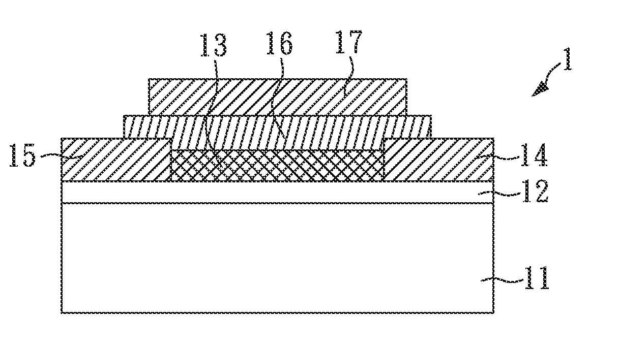
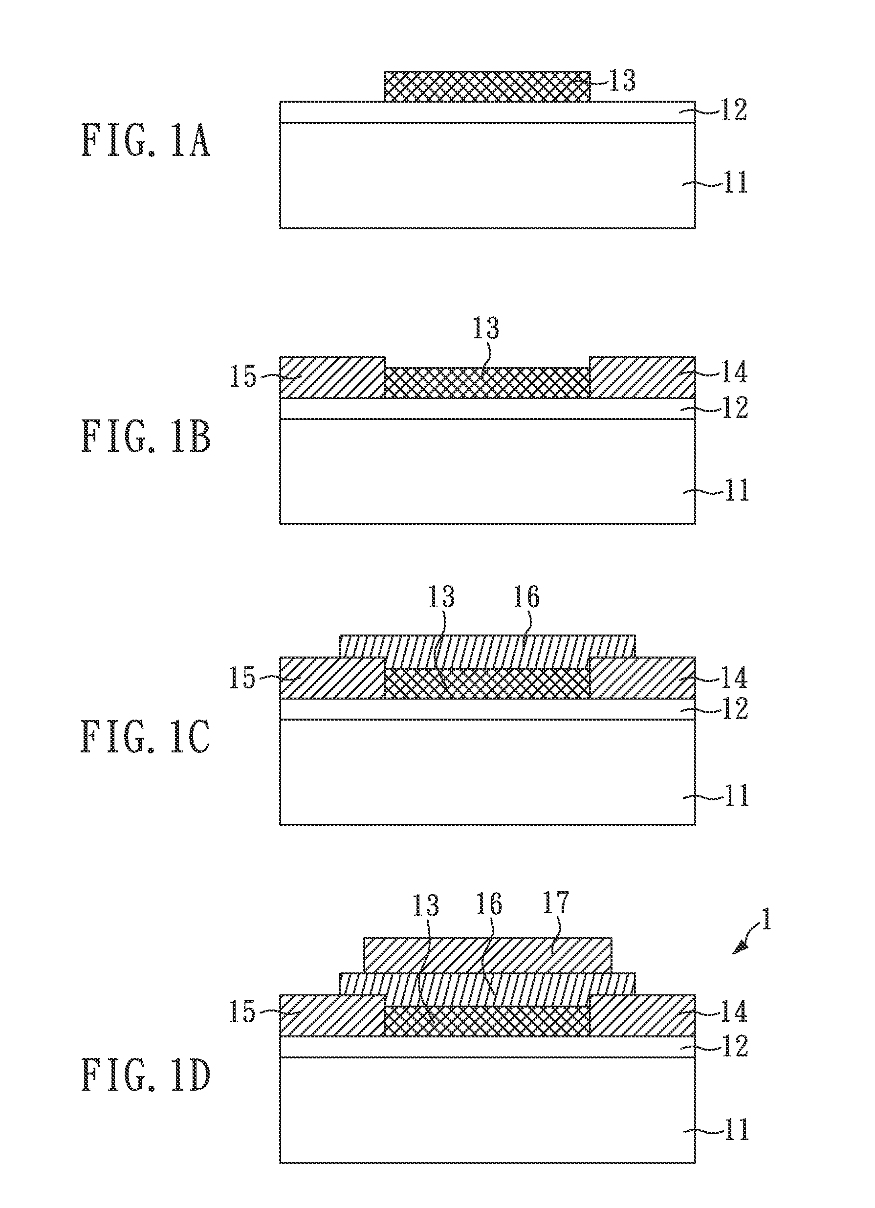
[0040]As illustrated in FIG. 1, it is first provided a silicon substrate 11 (step A) comprising a surface having a silicon dioxide layer 12, and on the silicon substrate 11 herein there is a single-walled carbon nanotube thin film 13 of a thickness of about 200 nm as deposited by a ACCVD device. The pattern of the passage region on the single-walled carbon nanotube transistor (step B) is defined by a photolithography technique and an etching technique. Next, as shown in FIG. 1B, a metal electrode layer (20 nm of gold / 300 nm of titanium) having a drain electrode 14 and a source electrode 15 is formed by a metal deposition system and a lift-off lithography. Afterwards, a hafnium oxide layer (HfOx) 16 deposited to be of about 10 nm by a sputtering device is made an oxide gate electrode of the transistor, as illustrated in FIG. 1C (step C). Afterwards, photolithography and dry etching technique etch the hafnium oxide layer 16 to form a contact hole containing a drain electrode 14 and a ...

embodiment 2

[0045]An identical method of fabricating a top-gate type thin film transistor as disclosed in embodiment 1 described therein, but the oxygen flow rate of step D for oxygen annealing treatment is 300 sccm, in stead of 100 sccm.

embodiment 3

[0046]An identical method of fabricating a top-gate type thin film transistor as disclosed in embodiment 1 described therein, but the oxygen flow rate of step D for oxygen annealing treatment is 500 sccm, in stead of 100 sccm, and the duration is 60 minutes, in stead of 30 minutes.

[Control Group 1]

[0047]An identical method of fabricating a top-gate type thin film transistor as disclosed in embodiment 1 described therein, but the step D is precluded, and the oxygen annealing treatment is precluded.

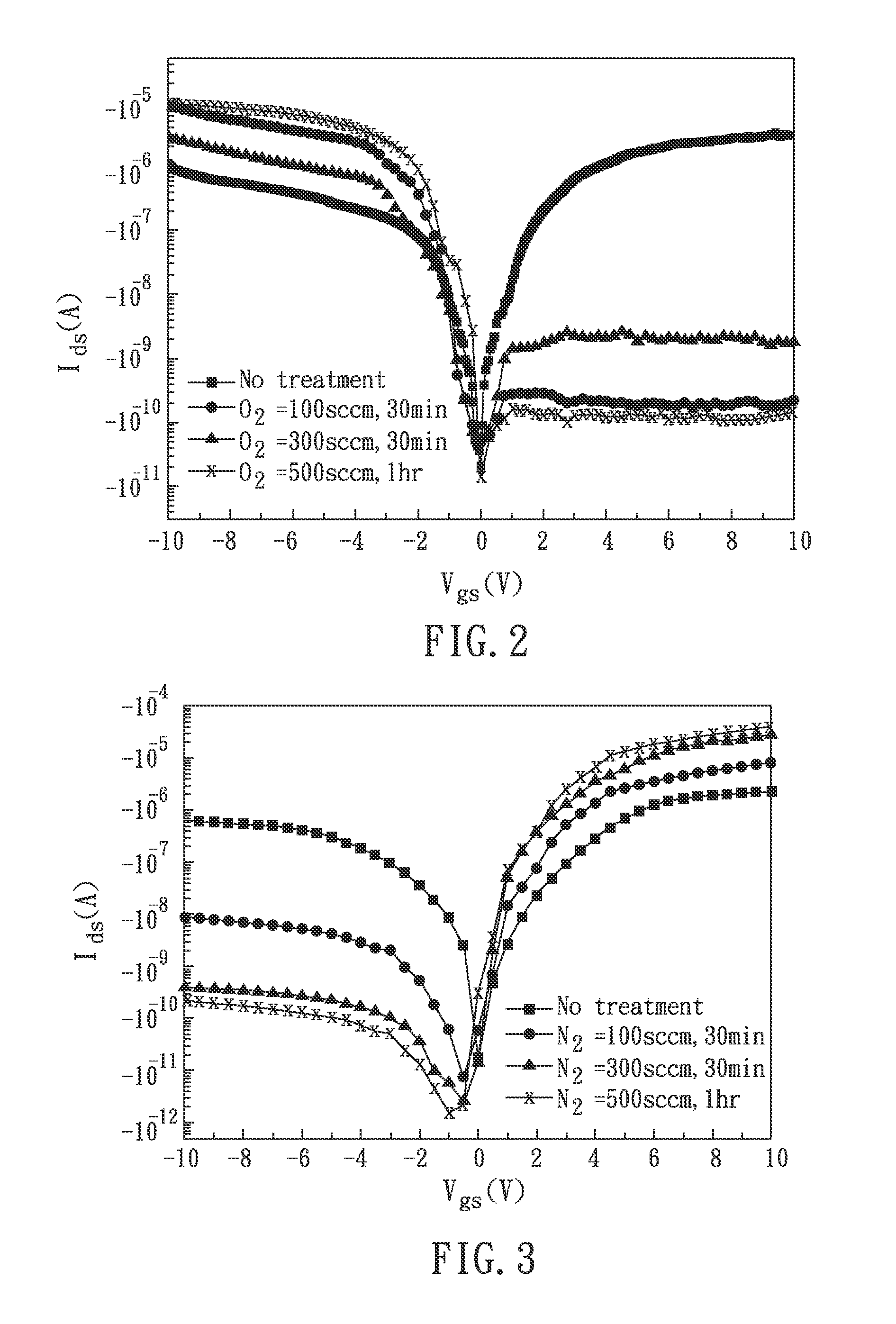
TABLE 1P-Type FETField-EffectOperationTransconductanceMobilityOn-off CurrentMeasurement(μ)(cm2 / Vs)RatioControl group 13.252.74~105  Oxygen flowing5.496.67105at 100 sccm,annealingduration for 30minutesOxygen flowing9.7172.57105~106at 300 sccm,annealingduration for 30minutesOxygen flowing10.6189.03106at 500 sccm,annealingduration for 60minutes

[0048]FIG. 2 shows the change in behavior of the transistor part property in response to changes in the hafnium oxide layer with different parametric co...


PUM


Abstract

A method of fabricating a thin film transistor (TFT) and a top-gate type thin film transistor are disclosed, the method of fabricating a TFT of the present invention comprises steps: (A) providing a substrate; (B) forming a source electrode, a drain electrode, and SWCNT (singled-walled carbon nanotubes) layer on the substrate, in which the source electrode and the drain electrode are spaced in a distance and the SWCNT layer is located between the source electrode and the drain electrode; (C) forming a gate oxide layer on the SWCNT layer; (D) annealing the gate oxide layer with oxygen or nitrogen gas; and (E) forming a gate electrode on the gate oxide layer; wherein the temperature used in the step (D) for annealing is a 500° C. to 600° C.

Description

BACKGROUND OF THE INVENTION[0001]1. Field of the Invention[0002]The present invention relates to a top gate thin film transistor and a method for fabricating the same. More particularly, the invention relates to a fabrication method subjecting single-walled carbon nanotubes in channeling layers.[0003]2. Description of Related Art[0004]Waves of study for synthesis and application of carbon nanotube found its root since its discovery in 1993. Of particular note with regard to its technology development is the Maruyama research team of Tokyo University of Japan, it was the first one to utilize alcohol catalytic chemical vapor deposition (ACCVD) to produce high-purity single-walled carbon nanotube. The nanotube resulting from this treatment process enjoys excellent electrical conductivity, simple manufacturing method, interpretability with photolithography and others, all of which has long drawn heavy attention from the scholarly community.[0005]Alternatively, in response to the current...

Claims


Application Information

Patent Timeline
IPC IPC(8): H01L29/772H01L21/336B82Y40/00B82Y99/00
CPCH01L51/0048B82Y10/00H01L51/0541H01L51/0525H10K85/221H10K10/472H10K10/464
Inventor GAU, CHIESHIAU, SHIUAN-HUACHENG, BAI-SHENG
Owner NAT CHENG KUNG UNIV
Why Eureka
Try Eureka