Laminate, method for producing same, and functional element using same

a technology of laminate and functional elements, applied in the direction of conductive layers on insulating supports, instruments, natural mineral layered products, etc., can solve the problems of low surface resistivity of transparent conductive films, low refractive index, and insufficient current diffusion in a film surface direction, so as to improve light extraction coefficient and improve refractive index , the effect of low solar light collection efficiency

Inactive Publication Date: 2012-12-27
SUMITOMO METAL MINING CO LTD +1
View PDF9 Cites 21 Cited by
  • Summary
  • Abstract
  • Description
  • Claims
  • Application Information

AI Technical Summary

Benefits of technology

[0043]As described above, matching of refractive index with the gallium nitride layer serving as a light emitting layer is obtained so that inner reflection of light on the interface between the gallium nitride layer and the transparent conductive film layer made of an oxide thin film that is mainly composed of titanium oxide and contains an additive element such as niobium can be prevented and the light-extraction coefficient can be improved.
[0044]Moreover, in the case

Problems solved by technology

Moreover, in the case when a gallium nitride layer is used for a light-emitting layer, a low surface resistivity is required for the transparent conductive film.
The reason for this is because the gallium nitride layer has an electrical characteristic in that the current diffusion in a film surface direction is not sufficient.
In this manner, since the ITO film is a material whose carrier concentration is extremely increased by tin serving as a dopant, a problem arises in which in an atte

Method used


Image

  • Laminate, method for producing same, and functional element using same
  • Laminate, method for producing same, and functional element using same
  • Laminate, method for producing same, and functional element using same

Examples


example 1

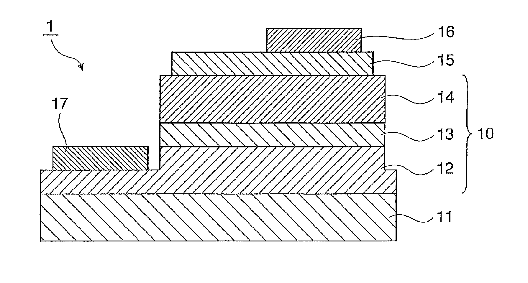
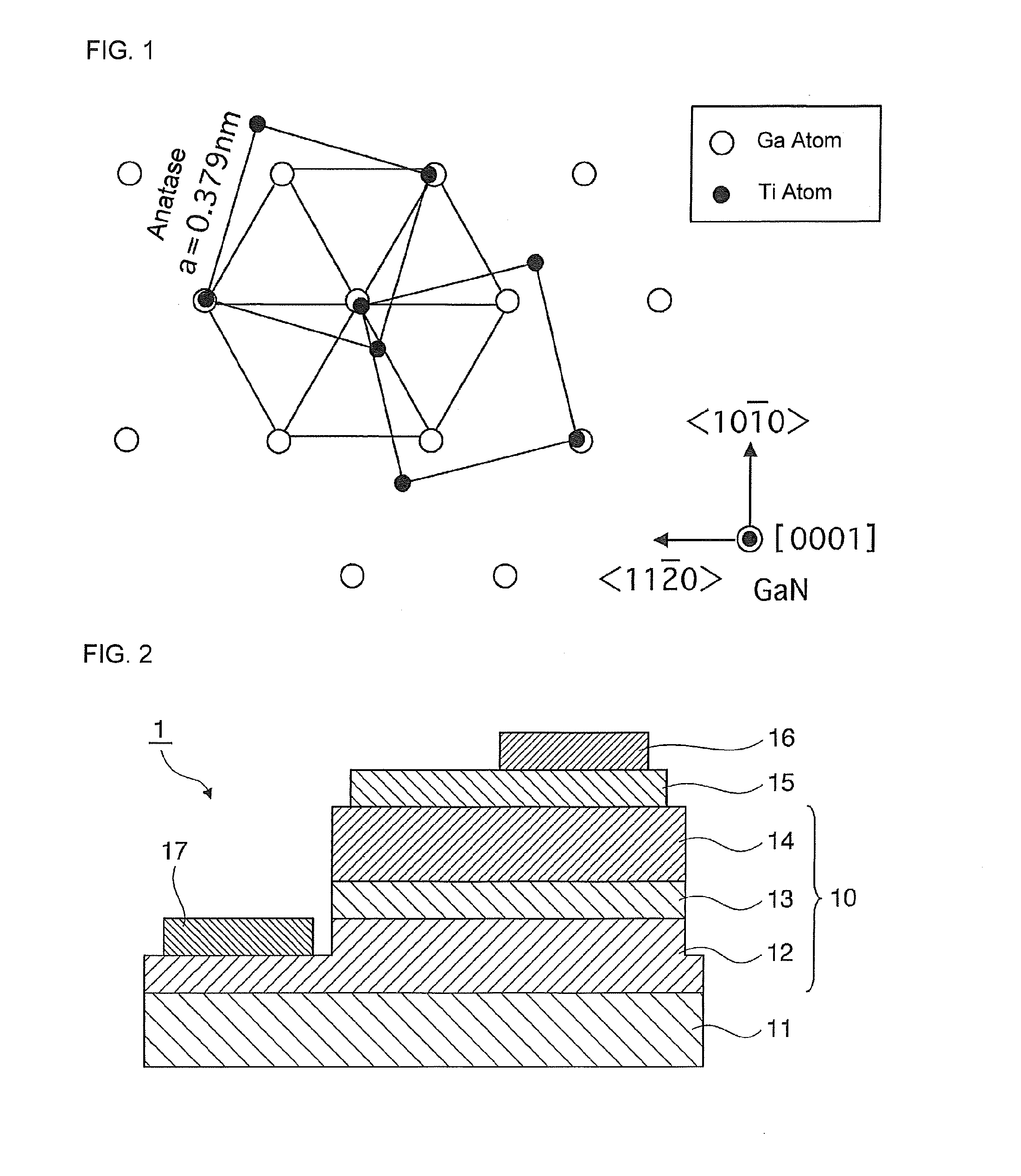
[0129]On a glass substrate, a buffer layer made of a gallium oxide thin film was formed, and a transparent conductive film layer, mainly composed of titanium oxide, containing niobium was formed thereon. In each of the film forming processes, a helicon-wave excitation plasma sputtering device (made by Sanyu Electron Co., Ltd.) was used.

[0130]As the glass substrate, an AN 100 substrate made by Asahi Glass Co., Ltd., with a thickness of 1.1 mm, was used. As the target, a gallium oxide sintered-material target having a diameter of 50 mm and a thickness of 6 mm and a niobium-added titanium oxide sintered-material target (made by Sumitomo Metal Mining Co., Ltd.) were used. Here, the content of niobium was 5.7% by atom in atomic ratio represented by Nb / (Ti+Nb).

[0131]First, a gallium oxide thin film was formed.

[0132]The inside of a chamber in a sputtering device was evacuated to a vacuum degree of 5×10⁻³ Pa or less, and this state was maintained, and after having been confirmed that the su...

example 2

[0136]The same processes as those of example 1 were carried out except that the buffer layer was changed to an oxide thin film composed of gallium, indium and oxygen so that a laminate film was formed.

[0137]As the target, an oxide sintered-material target, composed of gallium, indium and oxygen, having a diameter of 50 mm and a thickness of 6 mm (made by Sumitomo Metal Mining Co., Ltd.) was used. Here, the content of indium of this target was 5% by atom in atomic ratio represented by In / (Ga+In).

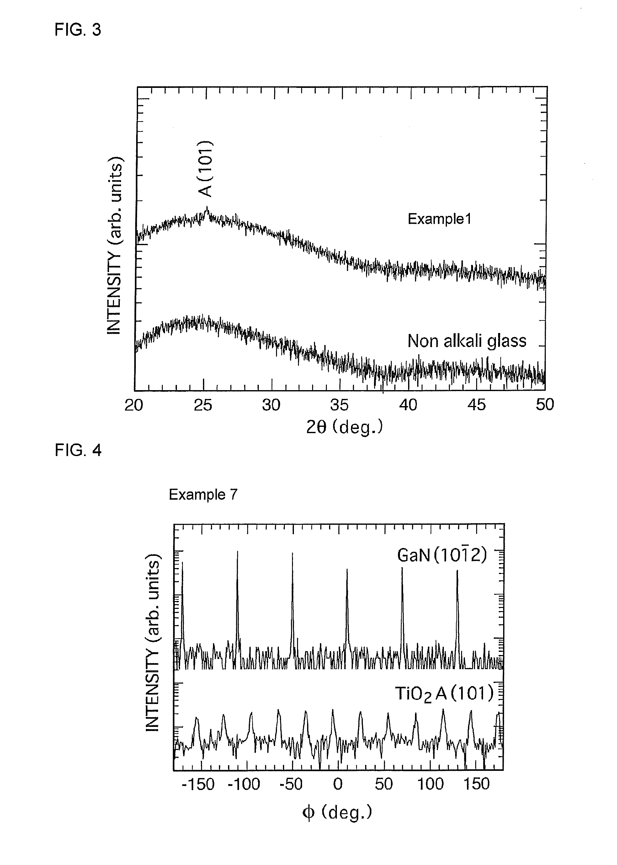
[0138]The resulting transparent conductive film had a specific resistivity of 4.5×10⁻⁴ Ω·cm and a refractive index of 2.5 at a wavelength of 460 nm, which were virtually the same level as that of example 1.

[0139]As a result of measurements on the crystallinity of the film by X-ray diffraction measuring method, the film was confirmed to be a crystalline film made of only an anatase phase as in the case of example 1. Additionally, since no diffraction peaks were confirmed with respect to the ga...

example 3

[0140]The same processes as those of example 1 were carried out except that the buffer layer was changed to an oxide thin film composed of gallium, indium, aluminum and oxygen so that a laminate film was formed.

[0141]As the target, an oxide sintered-material target, composed of gallium, indium, aluminum and oxygen, having a diameter of 50 mm and a thickness of 6 mm (made by Sumitomo Metal Mining Co., Ltd.) was used. Here, the content of indium of this target was 5% by atom in atomic ratio represented by In / (Ga+In+Al), and the content of aluminum was 1% by atom in atomic ratio represented by AI / (Ga+In+Al).

[0142]The resulting transparent conductive film had a specific resistivity of 5.4×10⁻⁴ Ω·cm and a refractive index of 2.5 at a wavelength of 460 nm, which were virtually the same level as that of example 1.

[0143]As a result of measurements on the crystallinity of the film by X-ray diffraction measuring method, the film was confirmed to be a crystalline film made of only an anatase p...


PUM

PropertyMeasurementUnit
Fractionaaaaaaaaaa
Fractionaaaaaaaaaa
Fractionaaaaaaaaaa

Abstract

Provided is a laminate which includes a transparent conductive film layer that is composed of an oxide thin film mainly composed of titanium oxide and contains an additional element such as niobium, and also contains an anatase phase having more excellent crystallinity and further has high refractive index and low resistivity by forming an optimal buffer layer on the substrate. Also provided are: a semiconductor light emitting element which comprises the laminate; and a functional element such as a solar cell, which includes the laminate.

Description

BACKGROUND OF THE INVENTION[0001]1. Field of the Invention[0002]The present invention relates to a laminate and a method for producing the same, and a functional element using the same. More specifically, the present invention concerns a laminate and a method for producing such a laminate, the laminate being configured in such a manner that a buffer layer, which is composed of an oxide thin film made of such as gallium oxide or an oxynitride thin film made of such as gallium oxynitride, is once formed on a substrate, and on the buffer layer, a transparent conductive film, which is mainly composed of titanium oxide and containing niobium or the like, and also made of a crystalline material containing an anatase phase, and further has high refractive index and low specific resistivity, is formed. The present invention also relates to a functional element provided with the above laminate, and in particular to a semiconductor light emitting element and a solar cell.[0003]2. Description ...

Claims


Application Information

Patent Timeline
IPC IPC(8): B32B9/04H01L31/02H01L33/26C23C14/34
CPCC23C14/083C23C14/086H01L31/022466H01L33/42Y10T428/265C23C14/0676C23C14/08C23C14/34C23C14/024Y02E10/52C23C14/3471H01L31/022483B32B9/00H01B5/14C23C14/06H01L31/04
Inventor CHICHIBU, SHIGEFUSAHAZU, KOUJINAKAYAMA, TOKUYUKITANAKA, AKIKAZU
Owner SUMITOMO METAL MINING CO LTD
Why Eureka
Try Eureka