
Wafer processing laminate, wafer processing member, temporary bonding arrangement, and thin wafer manufacturing method

a technology of wafer processing and wafers, applied in the direction of film/foil adhesives, synthetic resin layered products, transportation and packaging, etc., can solve the problems of insufficient strength and heat resistance to withstand, long time, and expensive tools, and achieve easy manufacturing, high heat resistance, and easy removal

Active Publication Date: 2013-05-02
SHIN ETSU CHEM IND CO LTD
View PDF6 Cites 43 Cited by
  • Summary
  • Abstract
  • Description
  • Claims
  • Application Information

AI Technical Summary

Benefits of technology

The patent describes a temporary adhesive layer that can be used in a variety of semiconductor film forming processes. The adhesive layer has high heat resistance, and can be applied even on a stepped wafer. It allows for the manufacturing of thin wafers of up to 50 μm, which can be easily removed from the support at room temperature. The use of a thin wafer is facilitated due to its ease of handling and fragility. The technical effects of this invention include the ability to manufacture thin wafers with high precision and ease of handling.

Problems solved by technology

Since the protective tape is based on an organic resin film, it is flexible, but has insufficient strength and heat resistance to withstand the TSV forming step and the step of forming interconnects on the back surface.
The former technology requires an expensive tool such as laser, a particular substrate (typically glass substrate) that is transmissive to laser light as the support, and a longer time of treatment per substrate.
The latter technology is simple because of control only by heat, but is applicable to a limited range because of instability at high temperatures in excess of 200° C. These temporary adhesive layers are not adequate to form a layer of uniform thickness on a heavily stepped substrate and to provide a complete bond to the support.
This method takes a very long time for removal and is applicable to the commercial manufacture process with difficulty.

Method used


Image

  • Wafer processing laminate, wafer processing member, temporary bonding arrangement, and thin wafer manufacturing method
  • Wafer processing laminate, wafer processing member, temporary bonding arrangement, and thin wafer manufacturing method
  • Wafer processing laminate, wafer processing member, temporary bonding arrangement, and thin wafer manufacturing method

Examples


synthesis example 1

Resin Synthesis Example 1

[0067]A four-necked flask was charged with 1,000 g (3.38 mol) of octamethylcyclotetrasiloxane and 0.24 g (0.0015 mol) of hexamethyldisiloxane and heated at a temperature of 110° C. Then, 4 g of 10 wt % tetrabutylphosphonium hydroxide siliconate was added to the flask whereupon polymerization was performed over 4 hours. The product was post-treated at 160° C. for 2 hours, obtaining dimethylpolysiloxane.

[0068]The product was analyzed by 29Si-NMR spectroscopy to determine the contents of D and M units. It was identified to be a dimethylpolysiloxane of the following structure consisting of 99.978% of D units and 0.022% of M units and having a degree of polymerization of about 9,000.

[0069]This dimethylpolysiloxane, 500 g, was dissolved in 500 g of hexane. This was poured into 2 L of acetone whereupon a precipitated resin was recovered. On subsequent removal of hexane in vacuum, there was obtained a dimethylpolysiloxane polymer having a Mw of 700,000 and containin...

synthesis example 2

Resin Synthesis Example 2

[0070]A four-necked flask was charged with 1,000 g (3.38 mol) of octamethylcyclotetrasiloxane and 0.93 g (0.003 mol) of tris(trimethylsiloxy)methylsilane and heated at a temperature of 110° C. Then, 4 g of 10 wt % tetrabutylphosphonium hydroxide siliconate was added to the flask whereupon polymerization was performed over 4 hours. The product was post-treated at 160° C. for 2 hours, obtaining dimethylpolysiloxane.

[0071]The product was analyzed by 29Si-NMR spectroscopy to determine the contents of D, M and T units. It was identified to be a branched dimethylpolysiloxane of the following structure consisting of 99.911% of D units, 0.067% of M units, and 0.022% of T units.

[0072]This branched dimethylpolysiloxane, 500 g, was dissolved in 500 g of hexane. This was poured into 2 L of acetone whereupon a precipitated resin was recovered. On subsequent removal of hexane in vacuum, there was obtained a dimethylpolysiloxane polymer having a Mw of 400,000 and containin...

synthesis example 3

Resin Synthesis Example 3

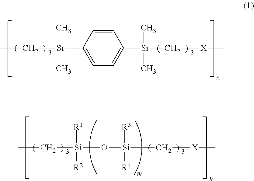
[0073]A flask equipped with a stirrer, thermometer, nitrogen purge line and reflux condenser was charged with 43.1 g of 9,9′-bis(3-allyl-4-hydroxyphenyl)fluorene (M-1), 29.5 g of organohydrogensiloxane having the average structural formula (M-3), 135 g of toluene, and 0.04 g of chloroplatinic acid and heated at 80° C. Then, 17.5 g of 1,4-bis(dimethylsilyl)-benzene (M-5) was added dropwise to the flask over one hour while the flask internal temperature rose to 85° C. At the end of dropwise addition, the reaction solution was aged at 80° C. for 2 hours. Toluene was distilled off, and instead, 80 g of cyclohexanone was added, obtaining a resin solution in cyclohexanone having a resin solid concentration of 50 wt %. The molecular weight of the resin in the solution was determined by GPC versus polystyrene standards, finding a Mw of 45,000. In formula (1), A=0.9 and B=0.1. To 50 g of the resin solution were added 5 g of hexamethoxymethylol melamine (Nikalac MW-39...


PUM

PropertyMeasurementUnit
temperatureaaaaaaaaaa
temperaturesaaaaaaaaaa
thicknessaaaaaaaaaa

Abstract

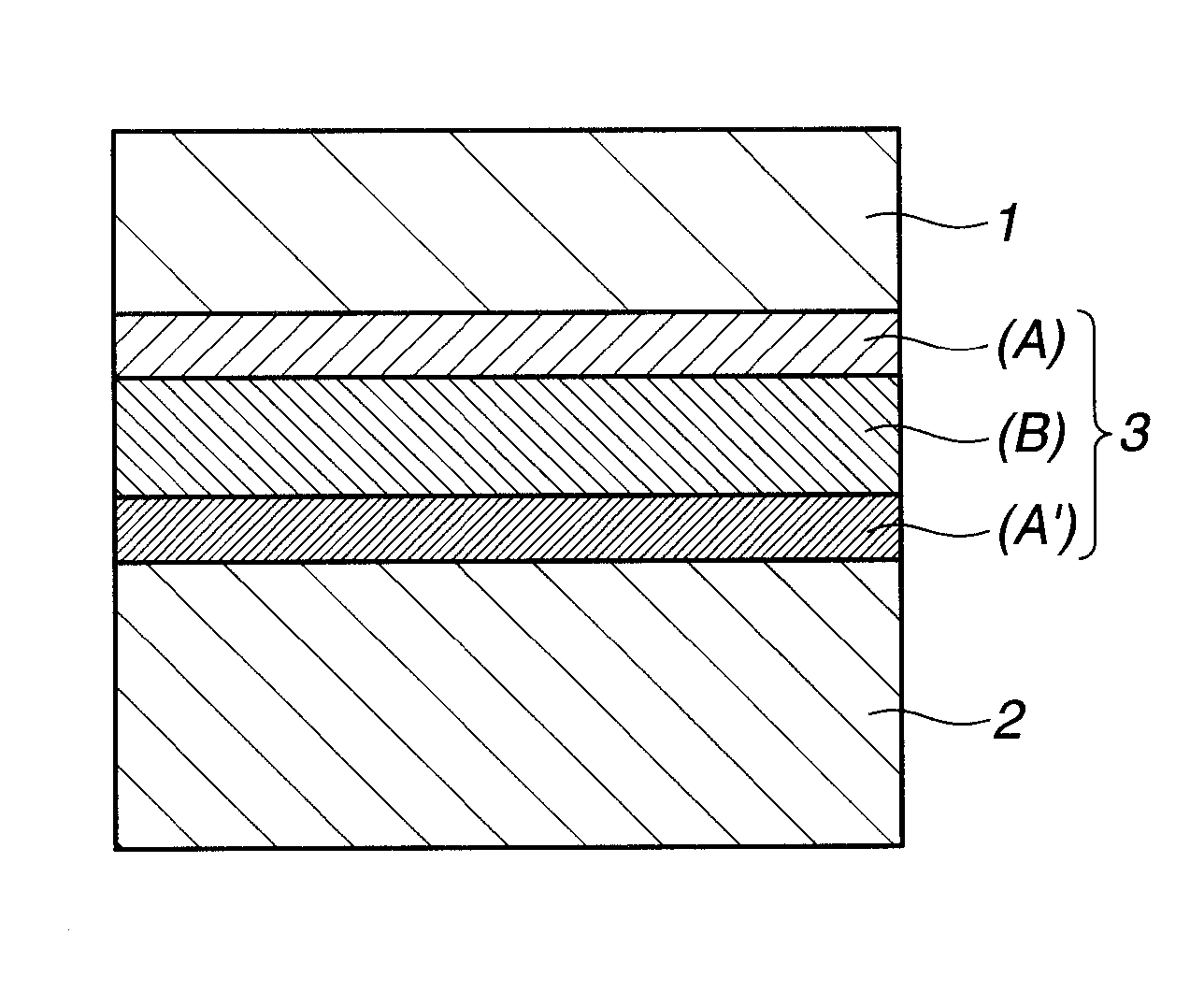
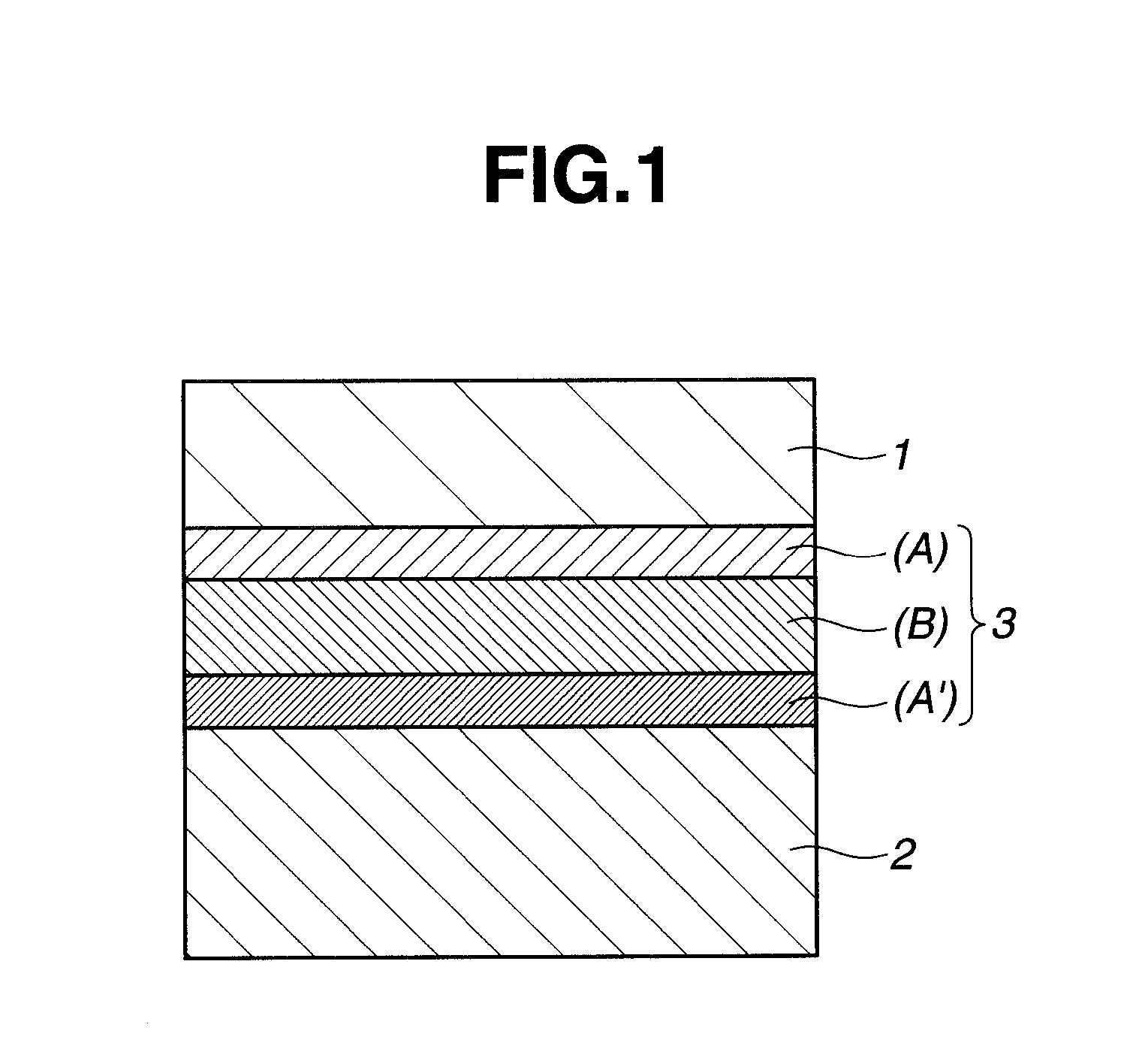
A wafer processing laminate is provided comprising a support, a temporary adhesive layer on the support, and a wafer laid on the temporary adhesive layer. The temporary adhesive layer has a trilayer structure consisting of a first bond layer (A) of thermoplastic organosiloxane polymer which is releasably bonded to the circuit-forming front surface of the wafer, a second bond layer (B) of thermosetting modified siloxane polymer which is laid on the first bond layer, and a third bond layer (A′) of thermoplastic organosiloxane polymer which is laid on the second bond layer and releasably bonded to the support.

Description

CROSS-REFERENCE TO RELATED APPLICATION[0001]This non-provisional application claims priority under 35 U.S.C. §119(a) on Patent Application No. 2011-236960 filed in Japan on Oct. 28, 2011, the entire contents of which are hereby incorporated by reference.TECHNICAL FIELD[0002]This invention relates to a wafer processing laminate, wafer processing member and temporary bonding arrangement allowing for processing the wafer, and a method for manufacturing a thin wafer.BACKGROUND ART[0003]Three-dimensional semiconductor packages become essential for a higher density and capacity. The 3D semiconductor packaging technology is by thinning semiconductor chips, and stacking them in multilayer structure while providing through-silicon via (TSV) interconnects. Fabrication of such packages requires the steps of thinning a substrate having a semiconductor circuit formed therein by grinding its non-circuit forming surface or back surface, and forming TSV and electrodes on the back surface. In the pr...

Claims


Application Information

Patent Timeline
Patent Type & Authority Applications(United States)
IPC IPC(8): C09J7/02B32B38/10B32B27/38B32B9/04B32B7/12
CPCC08G77/52Y10T428/2848C08G77/04C08G77/12C08G77/14C08L83/14H01L21/6835H01L2221/68327H01L2221/6834H01L2221/68381C09D183/14C08L63/00C09J183/04C09J183/14Y10T428/31663Y10T428/31511H01L21/20H01L21/02
Inventor KATO, HIDETOSUGO, MICHIHIROTAGAMI, SHOHEI
Owner SHIN ETSU CHEM IND CO LTD
Learn More