Electron Beam Processing With Condensed Ice

Active Publication Date: 2013-10-31
PRESIDENT & FELLOWS OF HARVARD COLLEGE
View PDF3 Cites 21 Cited by
  • Summary
  • Abstract
  • Description
  • Claims
  • Application Information

AI Technical Summary

Benefits of technology

[0010]Condensed, amorphous water ice can serve as a protective coating for detailed imaging and spatial mapping of a substrate surface while preventing contamination from reaching the surface, and then further serve as a resist for high resolution E-beam lithography. The properties of water ice allow direct application in a vacuum environment, conformal coating of complex three-dimensi

Problems solved by technology

For all of these features and materials, it is found that processing with an organic E-beam photoresist can produce residues that can contaminate devices and sensitize materials to contaminants, and can contaminate subsequent processes.
Indeed, electron transport studies of very clean as-grown SWCNTs have demonstrated that organic resist contamination can obscure the intrinsic electrical properties of SWCNTs.
Standard cleaning procedures for organic residue removal, such as oxygen plasma processes or highly oxidizing chemical treatments, have the unfortunate consequence that organic nanostructures, such as SWCNT and graphene, can themselves also be completely removed.
As a result, conventional E-beam photoresist materials are often incompatible with the materials and structures for which EBL is required

Method used


Image

  • Electron Beam Processing With Condensed Ice
  • Electron Beam Processing With Condensed Ice
  • Electron Beam Processing With Condensed Ice

Examples


example i

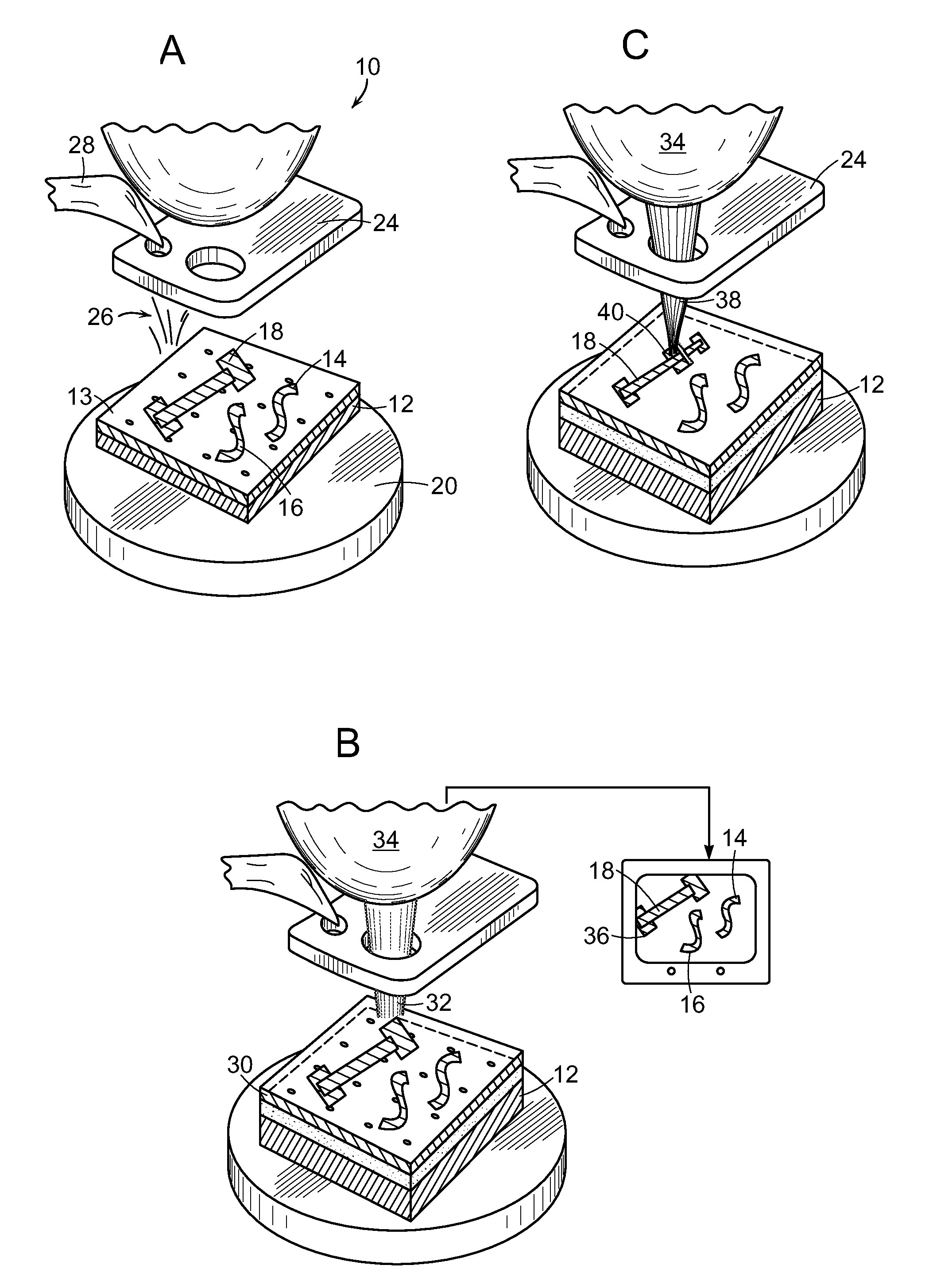
EBIL Fabrication Sequence for SWCNT FET Production

[0057]Molybdenum contact pads were provided on a silicon substrate having a blanket coating of a 500 nm-thick SiO2 layer and a 60 nm-thick Si3N4 layer. The substrate was etched with KOH to form a trench and ion beam milling was employed to form a slit in the trench. Iron catalyst pads for synthesis of single wall carbon nanotubes (SWCNTs) were patterned to lay near the focused ion beam-milled slits such that the SWCNTs would grow across the slits. Standard E-beam lithography and lift-off was carried out to overlap the catalyst pads with the preformed Mo pads, which could be held at ground potential. This geometry produced ideal conditions for imaging the SWCNTs by transmission electron microscopy.

[0058]After SWCNT growth, the sample was loaded into the SEM of the EBIL cluster tool of FIG. 2 via a door on the metal deposition chamber that served as a load lock which could be isolated from the main chamber with a butterfly valve. The s...

example ii

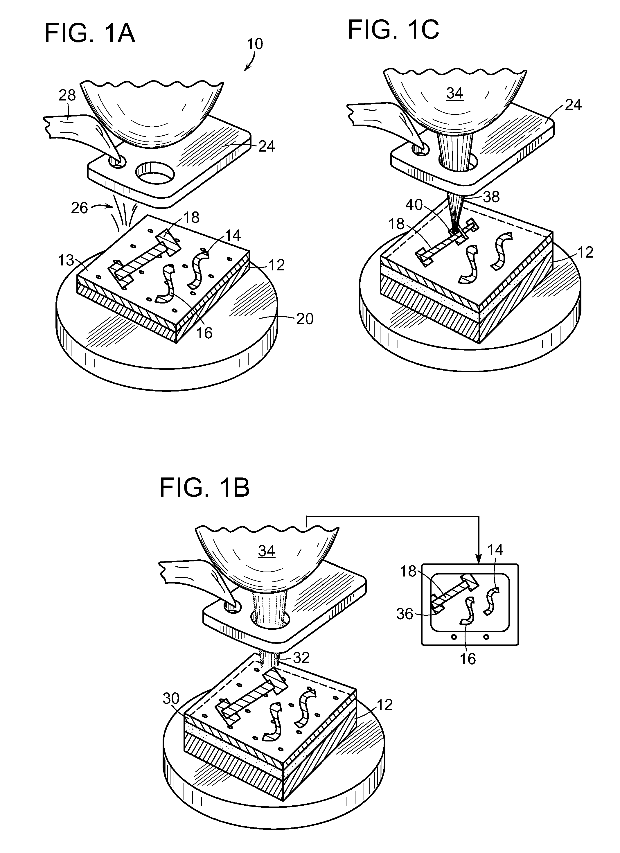
EBIL Fabrication Sequence for Three-Dimensional Structures

[0070]Photoresist spinning works very well for flat substrates and chips that are generally larger than about 3 mm×3 mm. Photoresist spinning does not, however, uniformly cover micro-scale, 3-D micromachined structures, such as probes for scanning probe microscopy. Vapor-deposited ice provided in the EBIL process sequence can be employed to cover 3-D structures easily. For example, as shown schematically in FIG. 4, the EBIL process enables production of a metallic coil on an AFM cantilever.

[0071]In this process, the following steps are conducted: an ice layer is condensed on the cantilever, E-beam mapping of the cantilever determines the coordinates for patterning of the ice layer, the layer is patterned by the E-beam, metal is deposited over the ice layer and the cantilever, and the ice layer and metal are lifted off, resulting in the metal remaining on the cantilever only at the locations corresponding to the ice layer patt...

example iii

EBIL Patterning of and Metal Deposition on Carbon Nanotubes

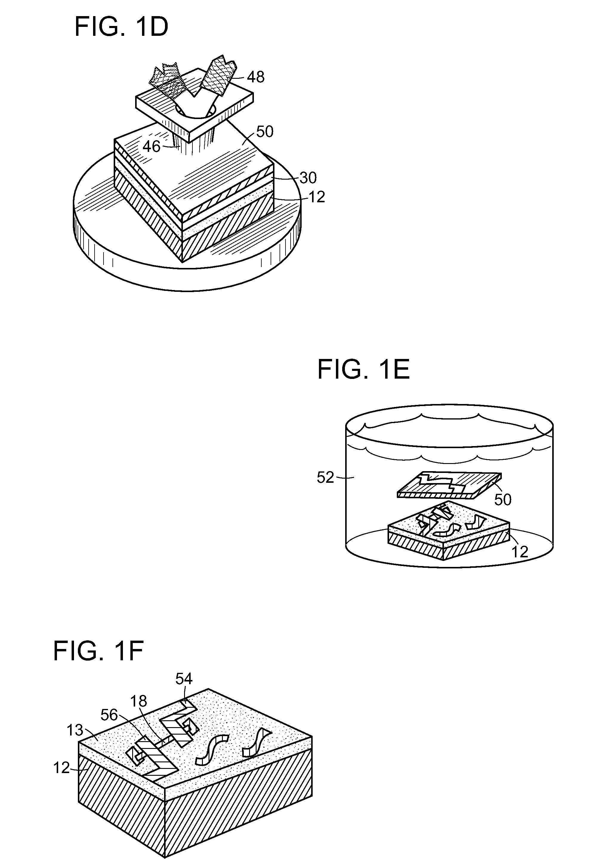
[0077]For many sensing and analysis applications, it is commonly preferred to dispose a carbon nanotube, such as a SWCNT as a freely suspended structure across, e.g., an aperture or trench. Such freely suspended SWCNTs are incompatible with conventional spin-coated resists not only because they are non-planar, but also because they are very fragile. With the EBIL process herein, there was fabricated electrically insulating nanoparticles coaxially surrounding titanium on a freely-suspended SWCNT.

[0078]SWCNTs were synthesized across a 1-μm-wide aperture in a silicon nitride membrane. The nanotubes were then coated with ice in the EBIL vacuum chamber, as in FIG. 1A. The ice-covered nanotubes were then imaged in the SEM, as in FIG. 1B, at a low E-beam dose that did not remove a significant amount of ice. Then nominally 25-nm-wide ice-free regions were patterned across the ice-coated SWCNTs to remove the ice at pattern sites. In ...


PUM

PropertyMeasurementUnit
Temperatureaaaaaaaaaa
Magnetic fieldaaaaaaaaaa
Pressureaaaaaaaaaa

Abstract

In a method for imaging a solid state substrate, a vapor is condensed to an amorphous solid water condensate layer on a surface of a solid state substrate. Then an image of at least a portion of the substrate surface is produced by scanning an electron beam along the substrate surface through the water condensate layer. The water condensate layer integrity is maintained during electron beam scanning to prevent electron-beam contamination from reaching the substrate during electron beam scanning. Then one or more regions of the layer can be locally removed by directing an electron beam at the regions. A material layer can be deposited on top of the water condensate layer and any substrate surface exposed at the one or more regions, and the water condensate layer and regions of the material layer on top of the layer can be removed, leaving a patterned material layer on the substrate.

Description

CROSS-REFERENCE TO RELATED APPLICATIONS[0001]This application claims the benefit of U.S. Provisional Application No. 61 / 407,508, filed Oct. 28, 2010, the entirety of which is hereby incorporated by reference.STATEMENT REGARDING FEDERALLY SPONSORED RESEARCH[0002]This invention was made with Government support under Contract No. 5R014G003703 awarded by the NIH. The Government has certain rights in the invention.BACKGROUND[0003]This invention relates generally to imaging and lithography for microfabrication processes, and more particularly relates to electron beam imaging and lithographic processes.[0004]Electron beam lithography (EBL or E-beam lithography) has become a critical tool for microelectronic fabrication processing and for nanoscience research. A wide range of applications, including microelectronics, nanoelectronics, optoelectronics, biological and biochemical sensing and analysis, and photovoltaic technologies all rely on EBL for the production of state-of-the-art systems....

Claims


Application Information

Patent Timeline
IPC IPC(8): G03F7/20
CPCG03F7/2059B81C2201/0143B81C1/00531H01L21/0331B81C2201/0159H01L22/12H01J37/3174H01J2237/004H01J2237/022H01J2237/2002G01N23/2251H01J2237/2803H01J2237/2809H01J2237/31796B82Y10/00B82Y40/00H10K71/20H10K85/221
Inventor BRANTON, DANIELHAN, ANPANGOLOVCHENKO, JENE A.
Owner PRESIDENT & FELLOWS OF HARVARD COLLEGE
Why Eureka
Try Eureka