

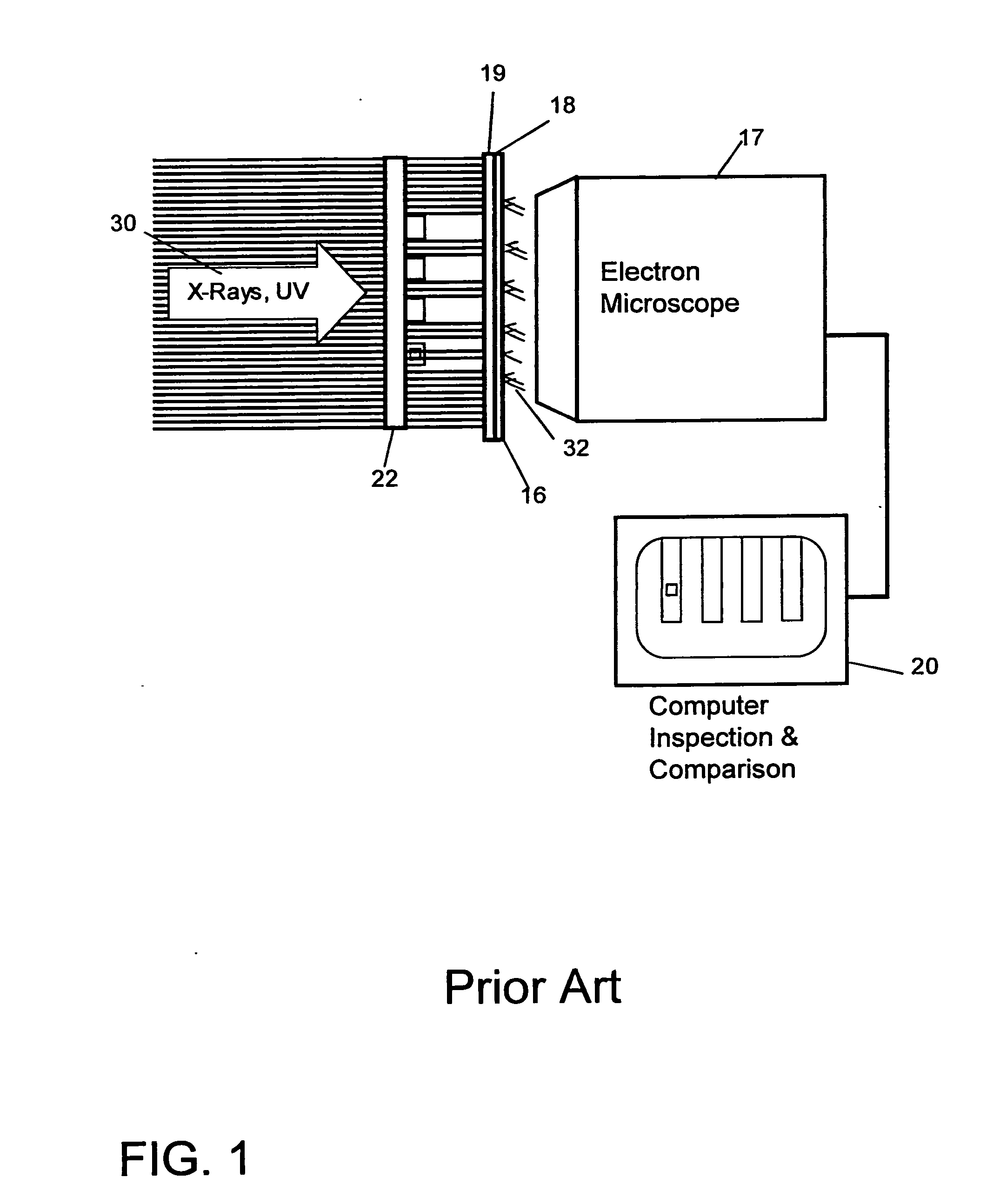
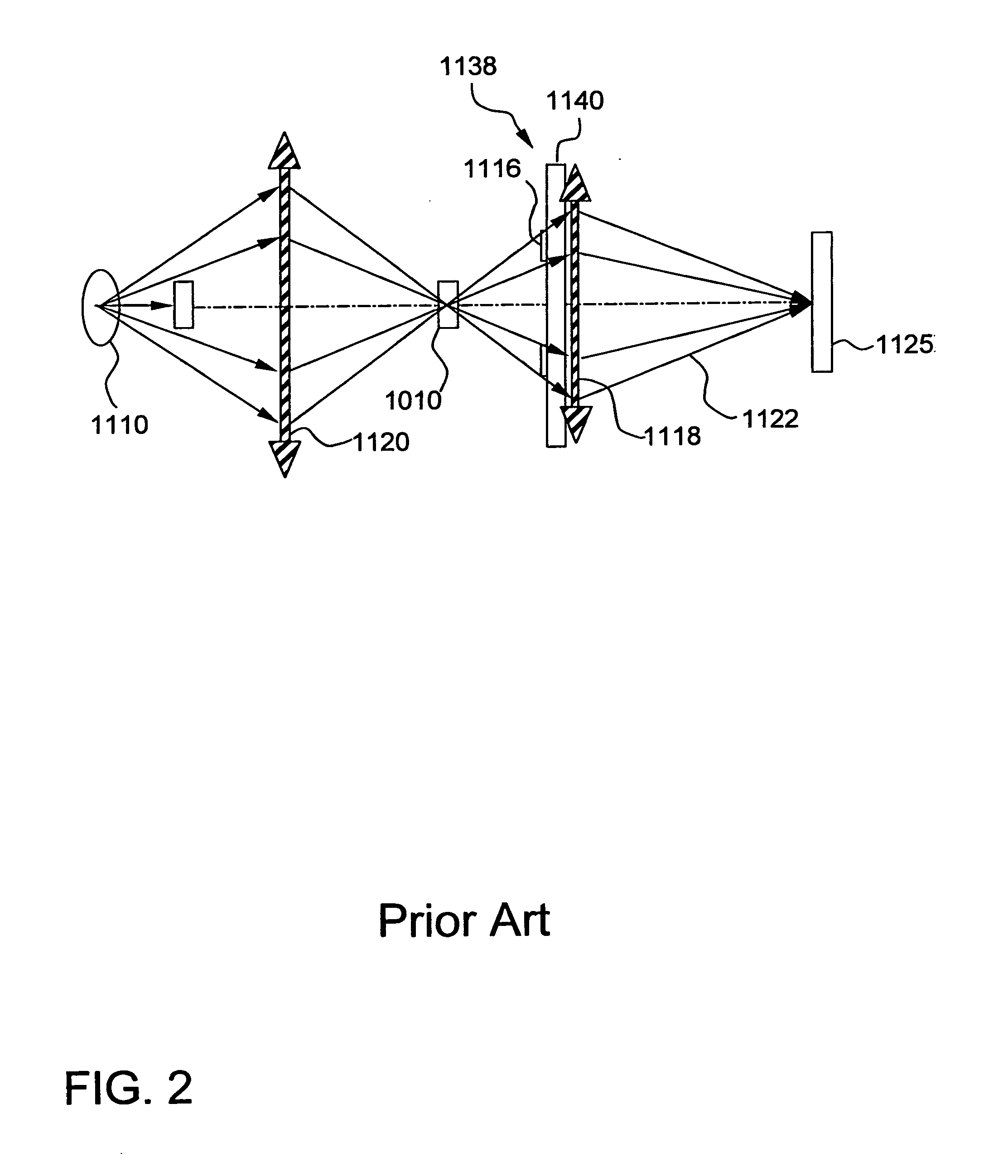
X-ray photoemission microscope for integrated devices
- Summary
- Abstract
- Description
- Claims
- Application Information
AI Technical Summary
Benefits of technology
Problems solved by technology
Method used
Image

Examples
first embodiment
of the Invention
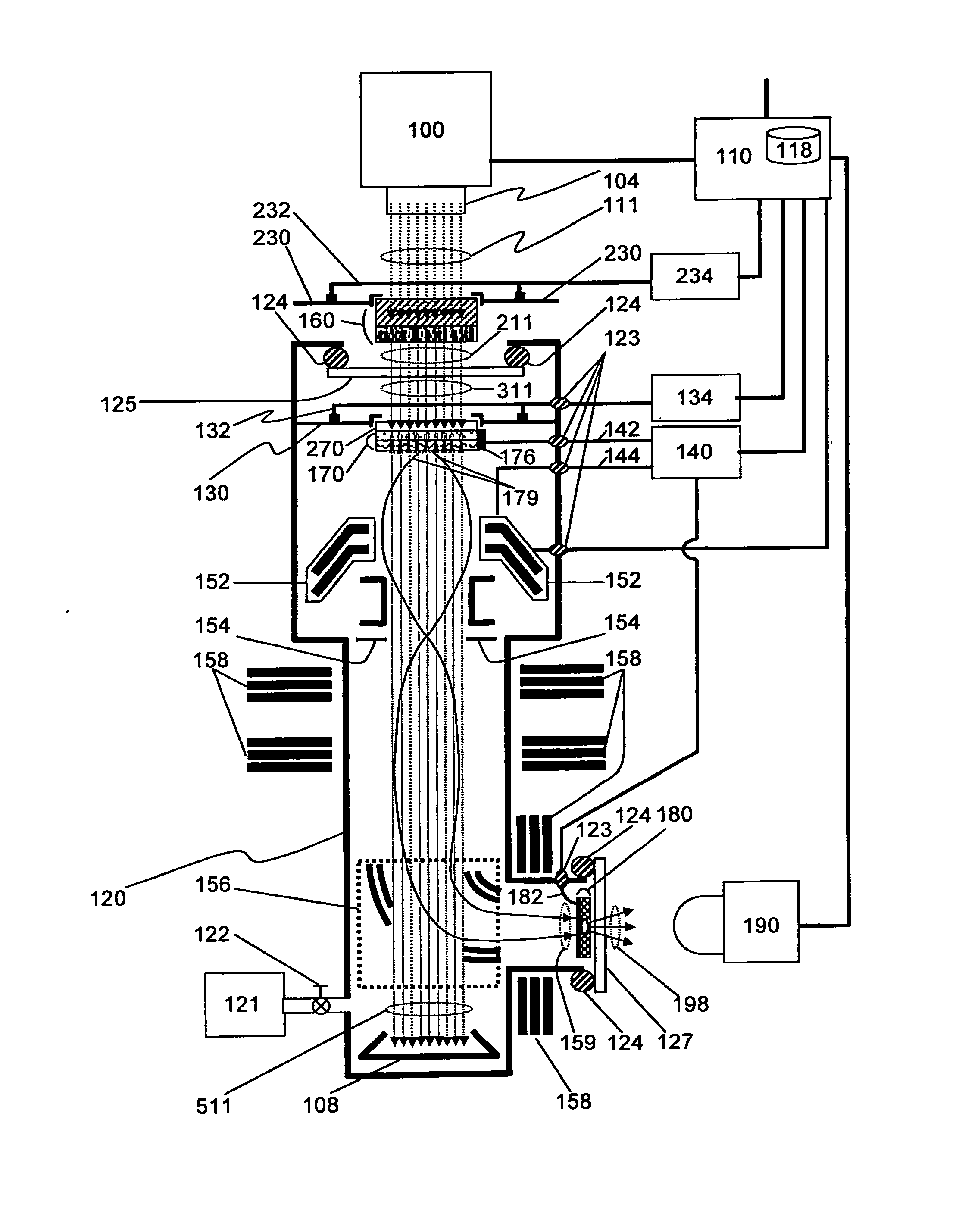
[0044]One embodiment of the apparatus according to the invention for the examination of an integrated device 160 is illustrated in FIG. 3 through FIG. 7. FIG. 3 illustrates a cross section view of the overall system. FIG. 4 illustrates a cross-section in detail of the integrated device 160 and photoemissive structure 170. FIG. 5 illustrates the x-ray energy absorption for copper, used in many integrated devices. FIG. 6 illustrates a cross section in detail of the image converter 180 and the imaging system 190. FIG. 7 illustrates a schematic of the various elements connected to the system controller 110.
[0045]Turning first to FIG. 3, the apparatus comprises a source of x-rays 100 and also comprises beam-shaping optics 104 which provide a beam of x-rays 111, directed onto the integrated device 160, with a predetermined energy (i.e. wavelength) spectrum and a predetermined angular distribution. The energy spectrum can be a broad emission spectrum, or filtered to have a ...
second embodiment
of the Invention
[0078]FIG. 8 and FIG. 9 illustrate another embodiment of an apparatus according to the invention. FIG. 8 illustrates a cross section view of the overall system, and FIG. 9 illustrates a cross-section in detail of the integrated device 160 and photoemissive structure 170.
[0079]As in the previously described embodiment of the invention, an x-ray source 100 produces a beam of x-rays 111 which are partially absorbed by the integrated device 160 under examination, forming a modified beams of x-rays 211.
[0080]As in the previously described embodiment of the invention, the integrated device 160 is mounted outside the vacuum chamber 120, using an external stage 230. In some embodiments of the invention, this external stage 230 will be fixed in place, and in others the external stage 230 may have external stage controls 232 to adjust position and orientation. Adjustment of the external stage controls 232 can be governed by an external stage controller 234, which is generally ...
third embodiment
of the Invention
[0089]FIG. 10 through FIG. 13 illustrate another embodiment of an apparatus according to the invention. FIG. 10 illustrates a cross-section view of the overall system, and FIG. 11 illustrates a cross-section in detail of the integrated device 160 and photoemissive structure 170. FIG. 12 and FIG. 13 each illustrate a cross-section in detail of the integrated device 160 and photoemissive structure 170 for two different variations of the embodiment.
[0090]As in the previously described embodiments of the invention, an x-ray source 100 produces a beam of x-rays 111. In this embodiment, however, the beam of x-rays directly enters the vacuum chamber 120 through the entrance window 125 without passing through the integrated device 160, becoming the interior unmodified beam of x-rays 411. The modifications that make the interior unmodified beam of x-rays 411 different from the incident beam of x-rays 111 are only due to absorption and scattering from the window 125.
[0091]In t...
PUM
 Abstract
Description
Claims
Application Information