
Method of growing group iii nitride crystals

a nitride crystal and group iii technology, applied in the field of group iii nitride crystals, can solve the problems of difficult to grow bulk gan crystals, high-power microwave transistors, and hinder the realization of high-end electronic devices

Active Publication Date: 2014-03-27
SEOUL SEMICONDUCTOR
View PDF4 Cites 17 Cited by
  • Summary
  • Abstract
  • Description
  • Claims
  • Application Information

AI Technical Summary

Benefits of technology

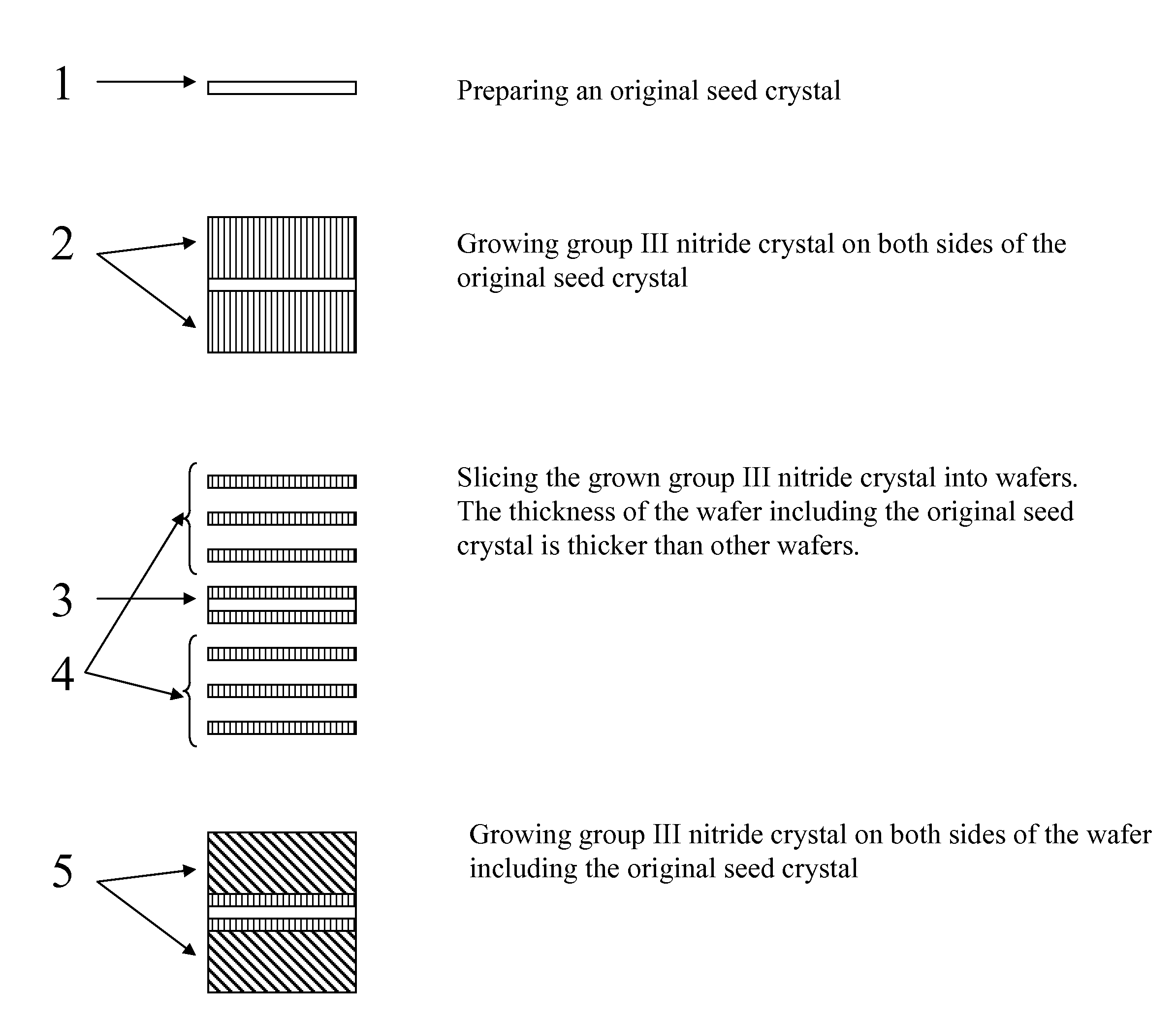
The patent presents a method for growing motley nitride crystals, specifically gallium nitride, using a process called ammonothermal. The method involves growing the crystals on both sides of a seed and then slicing the resulting ingot into thin wafers. Only the first-generation seed is allowed to be thicker than the others to prevent it from breaking. This thicker seed can then be used as a basis for further ammonothermal growth. Overall, this method allows for the efficient production of high-quality gallium nitride crystals.

Problems solved by technology

However, the majority of these devices are grown epitaxially on heterogeneous substrates (or wafers), such as sapphire and silicon carbide since GaN wafers are extremely expensive compared to these heteroepitaxial substrates.
The heteroepitaxial growth of group III nitride causes highly defected or even cracked films, which hinder the realization of high-end electronic devices, such as high-power microwave transistors.
However, due to the high melting point and high nitrogen vapor pressure at elevated temperature, it has been difficult to grow bulk GaN crystals.
HVPE is a vapor phase epitaxial film growth, thus difficult to produce bulk-shaped group III nitride crystals.
However, due to lack of natural crystal of group III nitrides, artificially grown crystals of group III nitrides must be used as seed crystals in the ammonothermal growth.

Method used


Image

  • Method of growing group iii nitride crystals
  • Method of growing group iii nitride crystals
  • Method of growing group iii nitride crystals

Examples


example 1

Old Technology

[0071]An ingot of GaN was grown on a GaN seed crystal with the ammonothermal method using polycrystalline GaN as a nutrient, supercritical ammonia as a solvent, and sodium (4.5 mol % to ammonia) as a mineralizer. The temperature was between 500 to 550° C. and pressure was between 170 and 240 MPa. The first-generation seed consisted of two GaN wafers with gallium polar surface mating together. The total thickness of the seed was 643 microns. The thickness of the crystal after growth was 6.6 mm and the surface area was approximately 100 mm2. A full-width half maximum (FWHM) of the X-ray diffraction from 002 plane was about 7001000 arcsec. Although the crystal was not characterized with an optical and electrical measurement, those characteristics are expected to be the typical one for bulk crystal of GaN. For example, photoluminescence or cathode luminescence is expected to show luminescence from band-edge emission at around 370 nm, blue emission at around 400 nm, and / or ...

example 2

This Invention

[0073]An ingot of GaN was grown on a GaN seed with the ammonothermal method using polycrystalline GaN as a nutrient, supercritical ammonia as a solvent, and sodium (4.5 mol % to ammonia) as a mineralizer. The temperature was between 500 to 550° C. and pressure was between 170 and 240 MPa. The first-generation seed consisted of two GaN wafers with gallium polar surface mating together. The total thickness of the seed was 919 microns. The thickness of the crystal after growth was 4.2 mm and the surface area was approximately 100 mm2. A full-width half maximum (FWHM) of the X-ray diffraction from 002 plane was about 700˜1000 arcsec. The lattice constant of the crystal was 51.86641 nm for c-lattice and 31.89567 nm for a-lattice. The lattice constant for GaN can change within 10% depending of growth conditions.

[0074]The crystal was sliced into c-plane wafers with a multiple wire saw using diamond slurry. The wire pitch was 1425 microns with wire thickness of 170 microns for...

example 3

Preparation of a Seed Composed of Two Layers

[0075]Several wafers of GaN, which are sliced from an ingot of GaN, are coated with metallic gallium on the gallium polar surface. The coating can be done by physical pressing of gallium foil on the wafer or vacuum evaporation. Since metallic gallium does not wet the surface of GaN wafer, the forming liquid phase of gallium is preferably avoided. With addition of some sort of flux, such as an organic material or alkali metals may act as a wetting agent, if liquid phase coating of gallium is attempted.

[0076]The first set of gallium-coated GaN wafers are placed on a glass slide in an array on edges with the gallium coating face up. This array becomes the first layer. Next, the second set of gallium-coated GaN wafers are placed on top of the first layer, making the second layer. The edges of the first layer do not match the edges of the second layer so that the arrays of GaN wafers are staggered with respect to one another and therefore are m...


PUM

PropertyMeasurementUnit
pressureaaaaaaaaaa
pressureaaaaaaaaaa
temperatureaaaaaaaaaa

Abstract

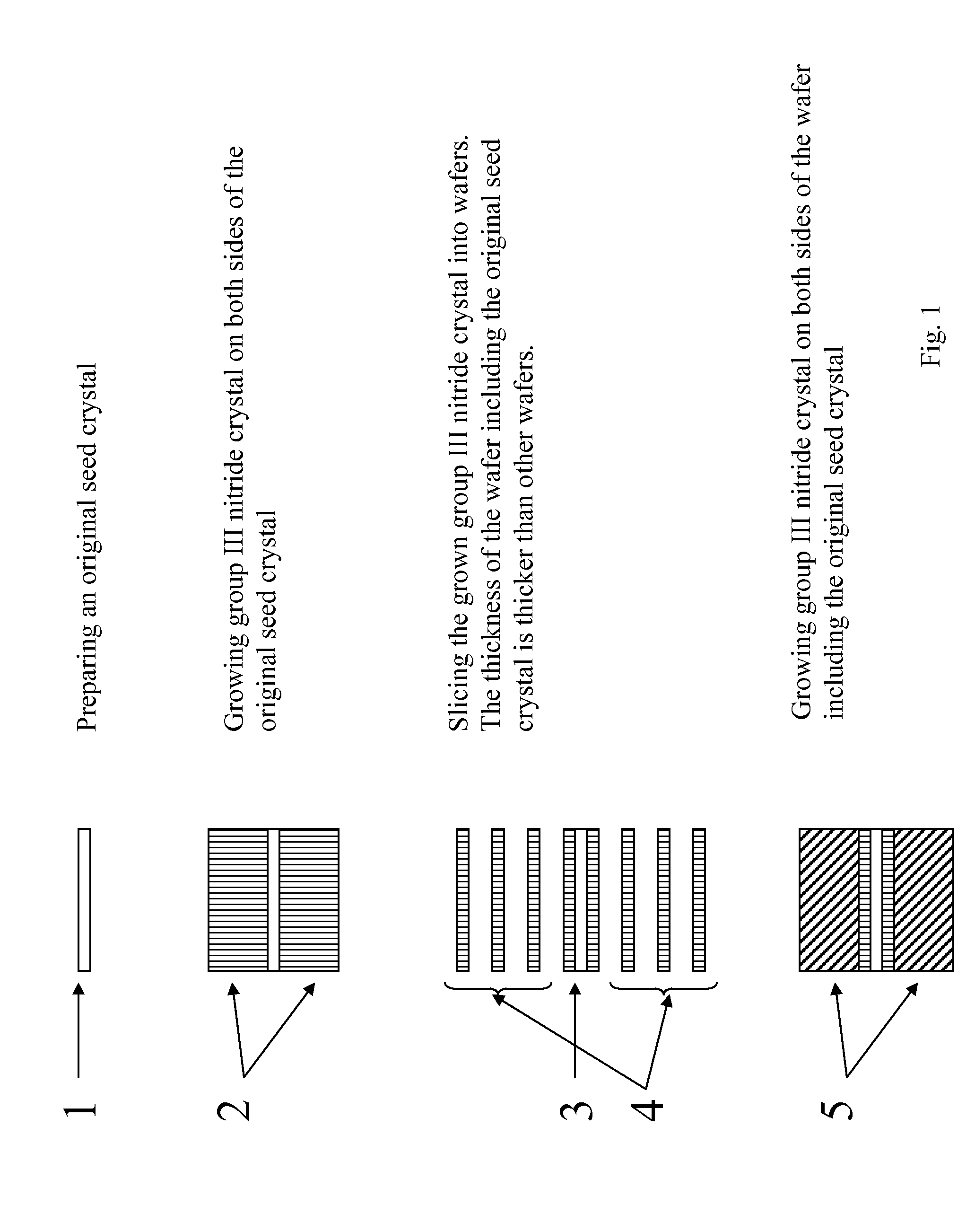
The present invention provides a method of growing an ingot of group III nitride. Group III nitride crystals such as GaN are grown by the ammonothermal method on both sides of a seed to form an ingot and the ingot is sliced into wafers. The wafer including the first-generation seed is sliced thicker than the other wafers so that the wafer including the first-generation seed does not break. The wafer including the first-generation seed crystal can be used as a seed for the next ammonothermal growth.

Description

CROSS REFERENCE TO RELATED APPLICATIONS[0001]This application claims priority to U.S. Patent App. No. 61 / 705,540 filed Sep. 25, 2012, by inventors Tadao Hashimoto, Edward Letts, and Sierra Hoff, entitled “METHOD OF GROWING GROUP III NITRIDE CRYSTALS”, which is incorporated by reference herein as if put forth in full below.[0002]This application is related to the following U.S. patent applications:[0003]PCT Utility Patent Application Serial No. US2005 / 024239, filed on Jul. 8, 2005, by Kenji Fujito, Tadao Hashimoto and Shuji Nakamura, entitled “METHOD FOR GROWING GROUP III-NITRIDE CRYSTALS IN SUPERCRITICAL AMMONIA USING AN AUTOCLAVE,” attorneys' docket number 30794.0129-WO-01 (2005-339-1);[0004]U.S. Utility patent application Ser. No. 11 / 784,339, filed on Apr. 6, 2007, by Tadao Hashimoto, Makoto Saito, and Shuji Nakamura, entitled “METHOD FOR GROWING LARGE SURFACE AREA GALLIUM NITRIDE CRYSTALS IN SUPERCRITICAL AMMONIA AND LARGE SURFACE AREA GALLIUM NITRIDE CRYSTALS,” attorneys docket ...

Claims


Application Information

Patent Timeline
Patent Type & Authority Applications(United States)
IPC IPC(8): H01L29/20C30B29/40C30B7/10
CPCH01L29/2003C30B29/403C30B7/105B28D5/045C30B29/406C30B29/64C30B33/06H01L21/02389H01L21/0254H01L21/02628Y10S117/902Y10T428/192C30B7/10C30B25/20H01L29/045H01L29/32
Inventor HASHIMOTO, TADAOLETTS, EDWARDHOFF, SIERRA
Owner SEOUL SEMICONDUCTOR
Learn More