Large area optical quality synthetic polycrystalline diamond window

a synthetic polycrystalline diamond and glass window technology, applied in the field of fabrication of optical quality synthetic polycrystalline diamond windows, can solve the problems of reducing reliant on relatively expensive feed gases. , to achieve the effect of increasing the exposure of dielectric window materials, high optical quality, and precise design tolerances

Active Publication Date: 2014-11-20
ELEMENT SIX TECH LTD
View PDF3 Cites 16 Cited by
  • Summary
  • Abstract
  • Description
  • Claims
  • Application Information

AI Technical Summary

Benefits of technology

[0053]Certain embodiments of the present invention have been realized by: (i) developing a particular microwave plasma reactor configuration; (ii) further modifying the microwave plasma reactor configuration to extremely precise design tolerances; and (iii) developing suitable process conditions for operating the microwave plasma reactor configuration to achieve fabrication of large synthetic polycrystalline diamond windows having extremely high optical quality.
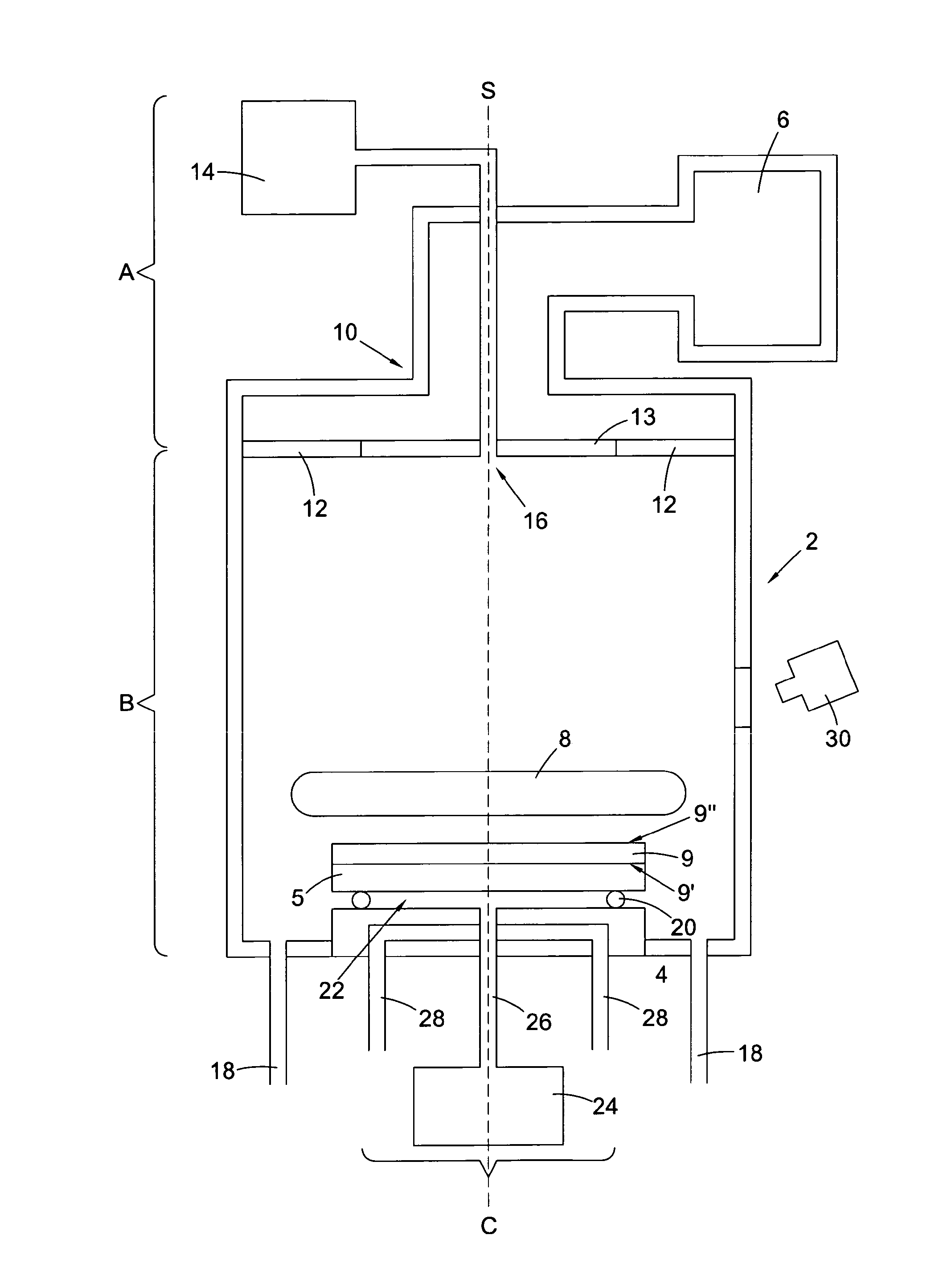
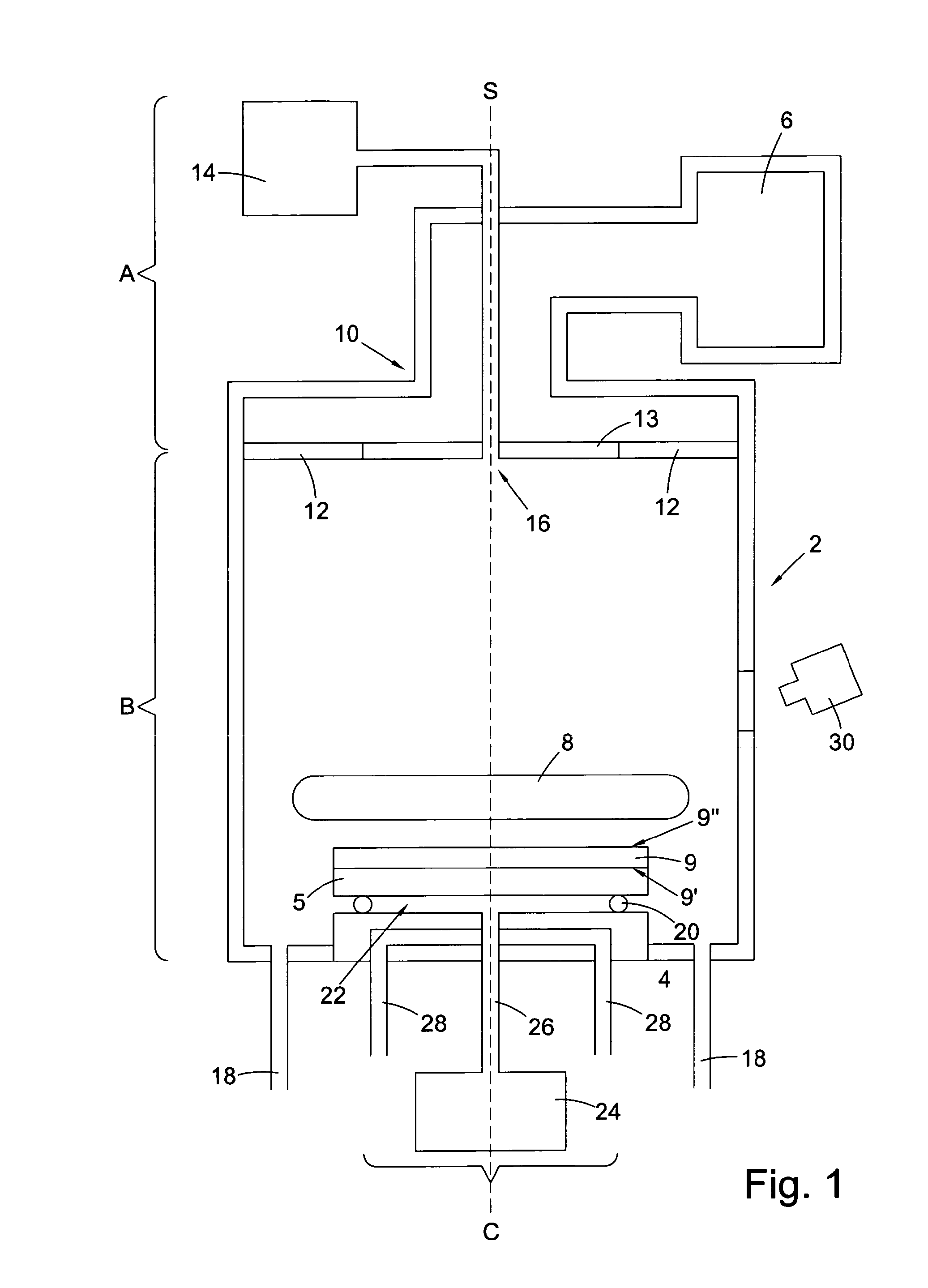
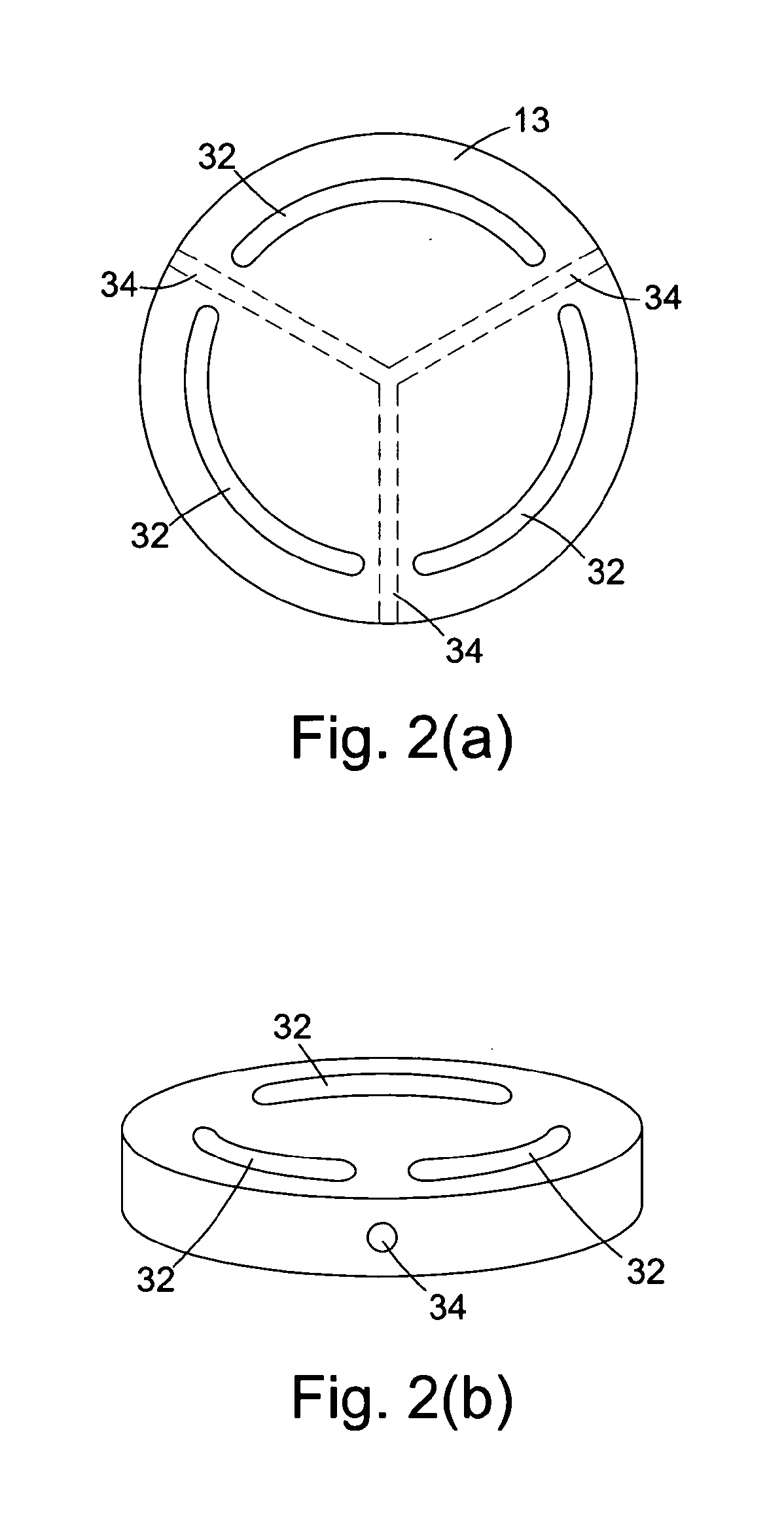
[0054]Having regard to point (i), the microwave plasma reactor is configured to couple both process gas, via one or more gas inlet nozzles, and microwaves, via an annular dielectric window, through a top plate of the plasma chamber towards a suitably temperature controlled substrate mounted in a base of the plasma chamber such that both process gas and microwaves are coupled into the plasma chamber in a rotationally symmetric manner and directed towards the substrate growth surface. Such a configuration has been found to be useful in allowing high gas flow rates, high process pressures, and high microwave power process conditions to be used for achieving good quality synthetic diamond growth at high growth rates with a suitably controlled nitrogen concentration. Furthermore, the provision of an annular dielectric window around a peripheral region of the top plate of the plasma chamber can reduce silicon transfer into the synthetic diamond material during growth when compared with alternatives such as the use of a bell jar, the use of a window spanning across a central portion of the plasma chamber, or an annular dielectric window disposed in a side wall of the plasma chamber, all of which increase exposure of the dielectric window material to a plasma region within the chamber.
[0055]Having regard to point (ii), it has been found that even utilizing such a configuration it is not possible to fabricate large area (≧120 mm diameter), thick (≧200 μm) windows of synthetic polycrystalline diamond having extremely high optical quality and no cracking. This problem has been traced to very minor misalignments in the microwave coupling configuration, the gas delivery system, and the substrate mounting and temperature control systems relative to the central rotational axis of symmetry of the plasma chamber. While minor misalignments do not manifest themselves in terms of a significant reduction in the quality of synthetic diamond material grown over smaller areas (e.g. ≦100 mm diameter), it has been found that when fabricating synthetic diamond material over larger areas (≧120 mm diameter) even very minor misalignments between components can detrimentally affect material quality, particularly around a peripheral region of the synthetic polycrystalline diamond wafer. As such, it has been found that the components, particularly the annular dielectric window, should be rotationally symmetric with each component having a rotational axis of symmetry lying within 0.2 mm of a central rotational axis of symmetry of the resonance cavity. Preferably other components such as the substrate holder and the one or more gas inlet nozzles should also be precisely configured and aligned. Such precise alignment, in combination with the previously described configuration in which process gas and microwaves are both coupled into the plasma chamber in an axial direction towards the substrate growth surface, allows high gas flow rates and high microwave power conditions to be achieved with a high degree of rotational symmetry which has been found to be critical for achieving the fabrication of large area, thick windows of synthetic polycrystalline diamond having extremely high optical quality.
[0056]Having regard to point (iii), it has been found that even utilizing the previously described precisely-aligned microwave plasma reactor configuration, the quality of polycrystalline diamond material around a peripheral region of the polycrystalline diamond wafer may not meet extremely high optical quality requirements. In particular, levels of impurities such as non-diamond carbon have been found to increase at a peripheral region of larger area wafers. This problem is exacerbated when also growing to larger thicknesses because as a synthetic polycrystalline diamond wafer grows, grain boundaries increase in size and this leads to an increase in the rate of impurity uptake within the grain boundaries. It has been found that this problem can be alleviated by increasing the hydrogen gas flow rate. It is considered that the concentration of atomic hydrogen required to selectively etch off non-diamond carbon from the substrate is lower at very large diameters and thus the efficiency of non-diamond carbon etching is reduced. It is believed that increasing the hydrogen gas flow rate directed towards the growth surface pushes more atomic hydrogen to peripheral regions of the polycrystalline diamond wafer thus increasing the rate at which non-diamond carbon is etched from the growth surface and improving the quality of the material in peripheral regions of the growing wafer. An alternative or additional solution is to provide a gas inlet nozzle array having a plurality of gas inlet nozzles directed towards the growth surface of the substrate and disposed over an area sufficiently large to ensure that a sufficiently large concentration of atomic hydrogen is provided in peripheral regions of a polycrystalline diamond wafer during growth. Yet another alternative or additional solution is to reduce the growth rate of the polycrystalline CVD diamond wafer to allow more time for non-diamond carbon to be etched from the growth surface. For example, the growth rate may be decreased as a thickness of the polycrystalline CVD diamond wafer increases by, for example, reducing the atomic concentration of carbon and / or the atomic concentration of nitrogen during growth of the polycrystalline CVD diamond wafer on the substrate.
[0057]By combining developments in reactor design, engineering tolerance control, and process design it has been possible to achieve fabrication of large synthetic polycrystalline diamond windows having extremely high optical quality.

Problems solved by technology

Methods that involve electrodes, such as DC arc plasmas, can have disadvantages due to electrode erosion and incorporation of material into the diamond.
Combustion methods avoid the electrode erosion problem but are reliant on relatively expensive feed gases that must be purified to levels consistent with high quality diamond growth.
Also the temperature of the flame, even when combusting oxy-acetylene mixes, is insufficient to achieve a substantial fraction of atomic hydrogen in the gas stream and the methods rely on concentrating the flux of gas in a localized area to achieve reasonable growth rates.
Perhaps the principal reason why combustion is not widely used for bulk diamond growth is the cost in terms of kWh of energy that can be extracted.
Compared to electricity, high purity acetylene and oxygen are an expensive way to generate heat.
Hot filament reactors while appearing superficially simple have the disadvantage of being restricted to use at lower gas pressures which are required to ensure relatively effective transport of their limited quantities of atomic hydrogen to a growth surface.
One problem with fabricating polycrystalline CVD diamond optical components is that during the CVD growth process impurities such as nitrogen, silicon and non-diamond carbon are incorporated into the diamond material as discussed below.
While nitrogen is advantageous for achieving commercially useful growth rates, incorporation of nitrogen into the synthetic diamond material can detrimentally affect the optical and thermal performance characteristics of the material.
Such silicon containing quartz components are exposed to extreme temperatures from the plasma in use and this can result in silicon from these components being incorporated into the synthetic diamond material.
However, this selective etching process does not usually remove all the deposited non-diamond carbon and such material therefore becomes incorporated into the CVD diamond material.
Uniformity is an issue in terms of spatial variations in the rate of impurity uptake across a growth surface and temporal variations in the rate of impurity uptake over a growth run.
For example, a non-uniform distribution of physical and / or chemical process parameters over the growth surface can lead to spatial variations in the rate of impurity uptake across a synthetic polycrystalline diamond wafer.
An increase in the size of grain boundaries as the synthetic polycrystalline diamond wafer grows thicker leads to an increase in the rate of impurity uptake within the enlarged grain boundaries which can result in an increasing concentration of impurities through the thickness of a synthetic polycrystalline diamond wafer.
In addition to the above described problems, variations in growth rate across a synthetic polycrystalline diamond wafer can lead to variations in impurity uptake.
Furthermore, variations in growth rate also cause variations in thickness which can lead to strain and cracking of synthetic polycrystalline diamond wafer on cooling after completion of the CVD growth process.
Variations in growth rate can be caused by non-uniformities in the plasma across the growth surface and non-uniformities in the temperature of the substrate on which the synthetic polycrystalline diamond wafer is grown.
However, the production of larger polycrystalline diamond wafers of high optical quality has proved problematic.
While it has been possible to fabricate larger polycrystalline diamond wafers, these have been of lower optical quality, particularly towards the periphery of the wafers.
Such wafers do not meet the requirements for certain commercial applications which require relatively thick, relatively large diameter synthetic polycrystalline diamond windows of extremely high optical quality.
However these sizes are not large enough for certain applications.

Method used


Image

  • Large area optical quality synthetic polycrystalline diamond window
  • Large area optical quality synthetic polycrystalline diamond window
  • Large area optical quality synthetic polycrystalline diamond window

Examples


example

[0181]A 140 mm diameter refractory metal carbide forming substrate suitable for synthesising polycrystalline CVD wafers was prepared using standard lapping and polishing processes to produce a surface with an Ra of 20-60 nm.

[0182]This substrate was introduced into a CVD reactor, and the synthesis process started. Reaction gases were flowed into the reactor at flows of 3500 / 43 / 43 sccm for Hydrogen / Methane / Argon. A controlled level of nitrogen was introduced to provide a concentration in the gas phase of 150 ppb, as quantified by optical emission spectroscopy.

[0183]The pressure in the chamber was kept at 185 Torr and the mean temperature of the substrate was adjusted to be 830° C. and was held at this point through the course of the growth run. The difference in substrate temperature from centre to edge was maintained at less than 30° C.

[0184]The synthesis process was terminated following a minimum diamond wafer deposition thickness of 1.0 mm. The diamond wafer was removed from the su...


PUM


Abstract

A polycrystalline chemical vapour deposited (CVD) diamond wafer comprising: a largest linear dimension equal to or greater than 125 mm; a thickness equal to or greater than 200 μm; and one or both of the following characteristics measured at room temperature (nominally 298 K) over at least a central area of the polycrystalline CVD diamond wafer, said central area being circular, centred on a central point of the polycrystalline CVD diamond wafer, and having a diameter of at least 70% of the largest linear dimension of the polycrystalline CVD diamond wafer: an absorption coefficient≦0.2 cm−1 at 10.6 μm; and a dielectric loss coefficient at 145 GHz, of tan δ≦2×10⁻⁴.

Description

FIELD OF INVENTION[0001]The present invention relates to the fabrication of optical quality synthetic polycrystalline diamond windows using a chemical vapour deposition (CVD) technique.BACKGROUND OF INVENTION[0002]Chemical vapour deposition (CVD) processes for synthesis of diamond material are now well known in the art. Useful background information relating to the chemical vapour deposition of diamond materials may be found in a special issue of the Journal of Physics: Condensed Matter, Vol. 21, No. 36 (2009) which is dedicated to diamond related technology. For example, the review article by R. S Balmer et al. gives a comprehensive overview of CVD diamond materials, technology and applications (see “Chemical vapour deposition synthetic diamond: materials, technology and applications” J. Phys.: Condensed Matter, Vol. 21, No. 36 (2009) 364221).[0003]Being in the region where diamond is metastable compared to graphite, synthesis of diamond under CVD conditions is driven by surface ki...

Claims


Application Information

Patent Timeline
Patent Type & Authority Applications(United States)
IPC IPC(8): C23C16/27G02B1/11C23C16/511
CPCC23C16/274G02B1/113C23C16/511
Inventor INGLIS, PAUL NICHOLASBRANDON, JOHN ROBERTDODSON, JOSEPH MICHAELMOLLART, TIMOTHY PETER
Owner ELEMENT SIX TECH LTD
Why Eureka
Try Eureka