Black silicon-based high-performance MEMS thermopile ir detector and fabrication method

Active Publication Date: 2015-06-18
ZHONGKE FUTURE OF CHIP MICROELECTRONICS TECH CHENGDU CO LTD
View PDF2 Cites 31 Cited by
  • Summary
  • Abstract
  • Description
  • Claims
  • Application Information

AI Technical Summary

Benefits of technology

[0039]7. The novel MEMS thermopile IR detector with high performance presented in this invention has features of excellent processing compatibility with CMOS fabrication, easy realization of device structure, easy

Problems solved by technology

As the materials of the substrates and the absorbers are conductive to some extent, such a direct overlapping method may influence the output signals of the thermopile IR detectors and ultimately affect device performance.
However, in the wavelength range of 1-12 μm, the average IR absorption efficiency that can be obtained from silicon nitride is only about 35%.
Besides, the thermopile IR detector with silicon nitride-based IR absorber cannot get a high responsivity and detection rate.
However, the preparation of gold-black involves metal evaporation, metallic nano-particle agglutination and other complicated processes.
Moreover, its compatibility with the CMOS process is poor and generally can only be produced on structure surfaces after completing process of device structures.
In view of this, the mass production of detectors with gold-black as the absorber is limited.
However, constrained by the resonanc

Method used


Image

  • Black silicon-based high-performance MEMS thermopile ir detector and fabrication method
  • Black silicon-based high-performance MEMS thermopile ir detector and fabrication method
  • Black silicon-based high-performance MEMS thermopile ir detector and fabrication method

Examples


Embodiment Construction

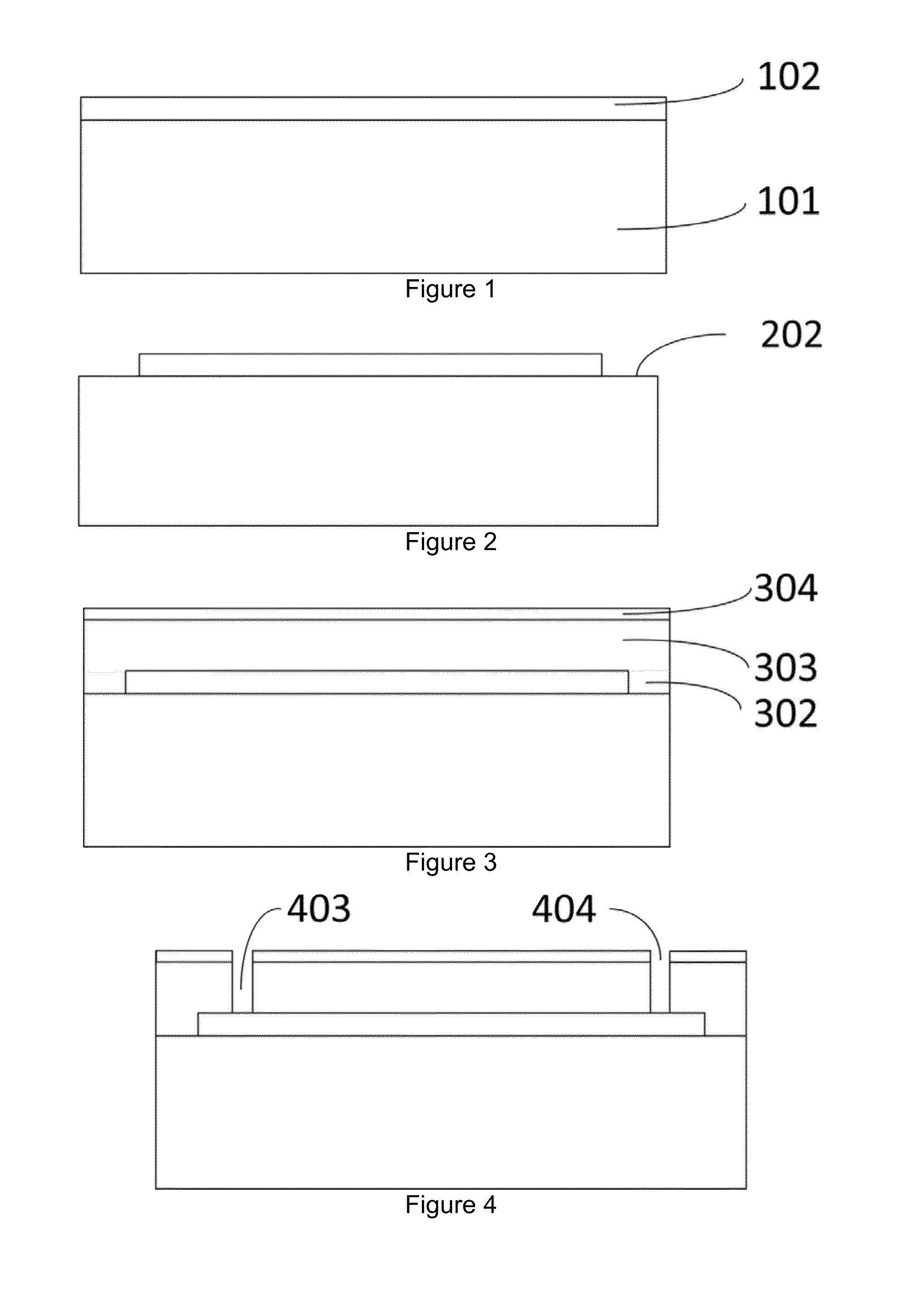
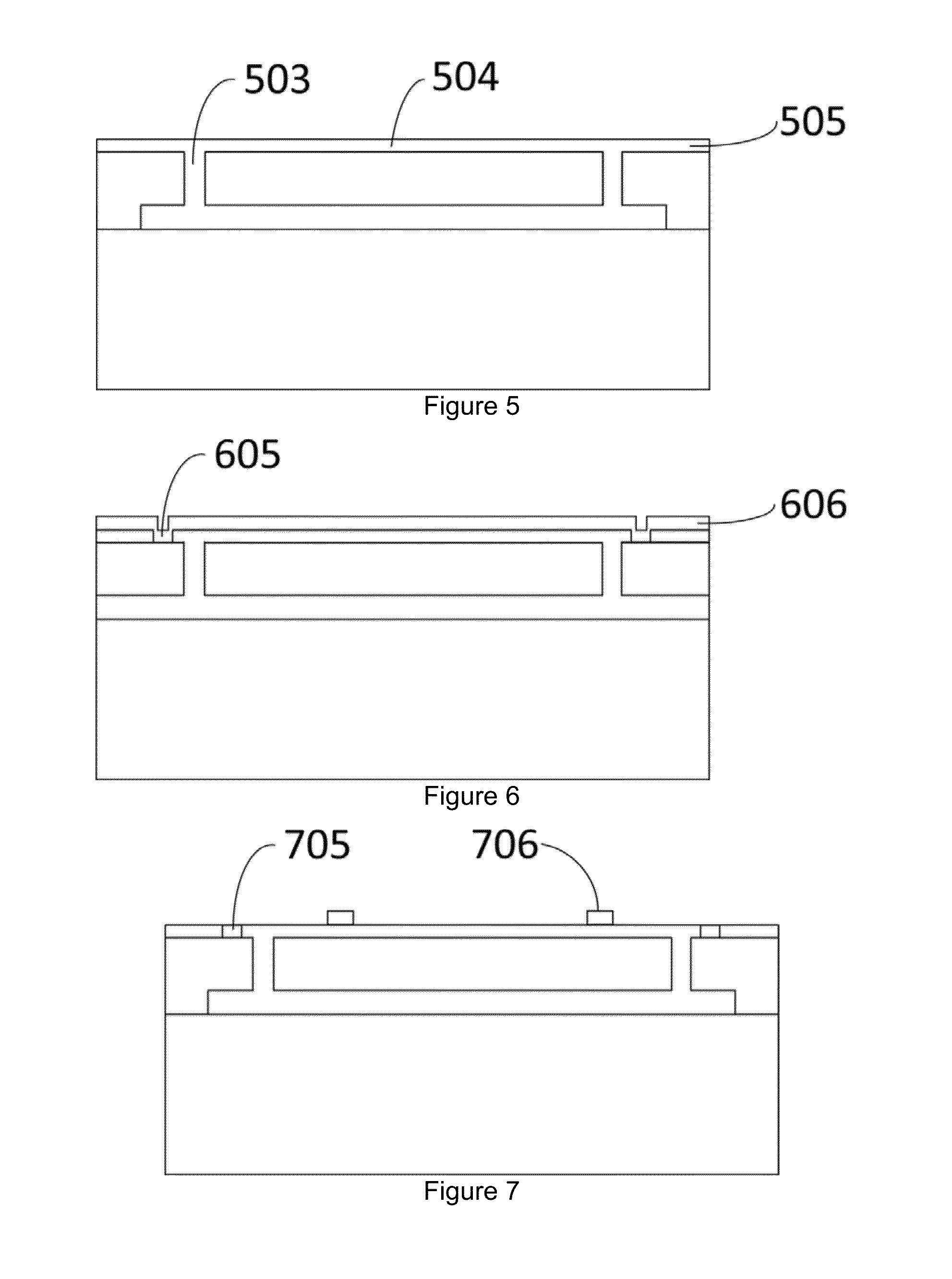
[0061]The invention will be further described with accompanying specific drawings and embodiments.

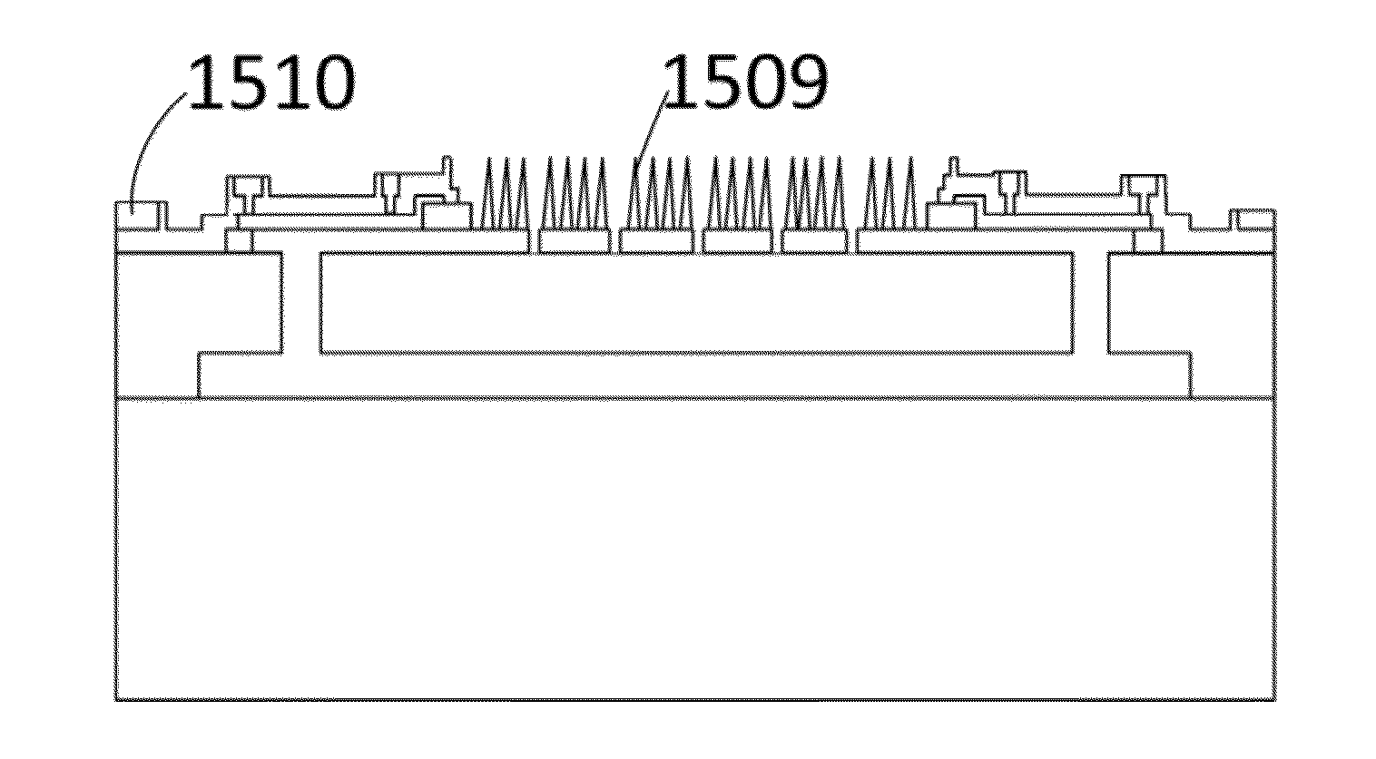
[0062]As shown in FIG. 17: the black silicon-based high-performance MEMS thermopile IR detector as described in this invention comprises a substrate 101; a releasing barrier band 2 on the substrate 101; the thermal isolation cavity 1403 constructed by and within the releasing barrier band 2; a black silicon-based IR absorber 1 right above the thermal isolation cavity 1403 and the black silicon-based IR absorber 1 is set above the releasing barrier band 2; a number of thermocouple strips are set around the lateral sides of the IR absorber 1.

[0063]The thermocouple strips around the black silicon-based IR absorber 1 are electrically connected in series. The thermopile being connected in series are equipped with electrodes 8, which are used to output signals. The terminals of the thermopile adjacent to the IR absorber form the hot junctions, while the terminals far away from the IR absorber...


PUM

PropertyMeasurementUnit
Structureaaaaaaaaaa
Electrical conductoraaaaaaaaaa
Metallic bondaaaaaaaaaa

Abstract

This invention involves structure and fabrication method of a black silicon-based MEMS thermopile IR detector. The high-performance black silicon-based MEMS thermopile IR detector includes a substrate; a releasing barrier band on the substrate; a thermal isolation cavity constructed by the releasing barrier band; a black silicon-based IR absorber located right above the thermal isolation cavity; a number of thermocouples are set around the lateral sides of the black silicon-based IR absorber. The thermopiles around the black silicon-based IR absorber are electrically connected in series thus to form a thermopile. Metallic electrodes are located beside the electrically-connected thermopiles for signal output. The cold junctions of the thermopile are connected to the substrate through the first thermal-conductive-electrical-isolated structures, the heat conductor is located at the lateral sides of the thermal isolation cavity. The hot junctions of the thermopile are in contact with the IR absorber through the second thermal-conductive-electrical-isolated structures, and the second thermal-conductive-electrical-isolated structures are located above the releasing barrier band. The structure of such detector is simple, and it is easy to implement and can also be monolithicly integrated. Such detector has high responsivity and detection rate, and is CMOS-compatible, thus can be used widely in a safe and reliable manner.

Description

FIELD OF THE INVENTION[0001]This invention involves an infrared (IR) detector and fabrication method and, especially, a black silicon-based high-performance MEMS thermopile IR detector and its fabrication method. The invention belongs to a technical field of MEMS IR detectors.BACKGROUND[0002]MEMS thermopile IR detector is a typical device in the field of sensing detection and one of the core components for constituting temperature sensor, root-mean-square converter, gas sensor, thermal flow meter and other sensor detectors. Moreover, small size thermopile IR detector can also be used for constructing IR focal plane arrays (FPA) and thus realizing IR imaging. Compared with IR detectors based on other operating principles (such as pyroelectric IR detectors and thermistor IR detectors etc.), thermopile IR detector has obvious comprehensive benefits of measurable constant radiant quantity, having no need to apply bias voltage or use chopper, and being more applicable to mobile applicati...

Claims


Application Information

Patent Timeline
IPC IPC(8): G01J5/12B81C1/00H01L35/34B81B7/02H01L35/32H01L35/22
CPCG01J5/12H01L35/32H01L35/22B81B2201/0278B81B7/02B81C1/00111H01L35/34G01J5/022H10N10/01H10N10/17H10N10/855
Inventor MAO, HAIYANGOU, WEN
Owner ZHONGKE FUTURE OF CHIP MICROELECTRONICS TECH CHENGDU CO LTD
Why Eureka
Try Eureka