Protective cover for a copper containing conductor

a protective cover and copper-containing technology, applied in the direction of photovoltaic energy generation, electrical equipment, basic electric elements, etc., can solve the problems of limited conductivity, high price, large area needed, etc., and achieve the effect of enhancing the reactivity and the deposition rate of si, minimizing process steps, and reducing the size of the protective cover

Inactive Publication Date: 2015-10-15
M4SI
View PDF1 Cites 4 Cited by
  • Summary
  • Abstract
  • Description
  • Claims
  • Application Information

AI Technical Summary

Benefits of technology

[0014]The use of a copper silicide as a surface layer in the invention, covered with a protective layer of an insulating silicon compound, results in a good surface protection. It is very well suitable for the provision of copper-containing conductors in solar cells, wherein a primary conductor typically connects the substrate surface to a contact or through-substrate via over a significant lateral distance. Herein, a good protection is more important than the ability of reopening the protective cover at many locations at high resolution, such as in integrated circuit manufacture. Moreover, the mentioned applications often require a low temperature process and this can be met with the present invention.
[0033]Suitably, the interface layer constitutes a plating base and the copper-containing conductor is deposited in an electrochemical process. This results in a low-cost process that is robust, suitable for creation of conductors of sufficient height and thickness to provide low resistance. Furthermore, the electrochemical process is a low-temperature process, which may be carried out at room temperature, but also at 80° C. or any intermediate temperature. In a further embodiment, the exposed surface extends on a top face of the conductor as well as to a side face hereof. This extension on both top face and side face, in combination with the presence of the interface layer acting as a diffusion barrier, results therein that the copper is essentially hermetically encapsulated. Therewith an optimum protection against diffusion of copper species into other layers and particularly the silicon substrate is prevented.

Problems solved by technology

Disadvantages of the use of such metal paste include its limited conductivity, the large area needed and a high price.
A disadvantage of such copper-containing conductors is that copper has a tendency to migrate, which may cause malfunctioning.
The migration is particularly problematic in the presence of semiconductor substrates, such as silicon substrates.
These damascene processes require plurality of lithographical steps, which result in a high cost price, and are therefore specific to the application in integrated circuits.
In solar cells the use of copper containing conductors is less widespread, even though the low cost price of electrochemical processes fits such applications.
There is however a second disadvantage in using copper that needs to be overcome, which is a protection of copper-containing conductors against corrosion and oxidation, leading f.i. to increased resistance of the conductors, failures due to open circuits and poor contacts to any underlying substrate, such as a semiconductor substrate.
These known protective covers suffer from either only short-term protection (OSP) or high material and processing costs (Sn, Ni—Au).

Method used


Image

  • Protective cover for a copper containing conductor
  • Protective cover for a copper containing conductor
  • Protective cover for a copper containing conductor

Examples


second embodiment

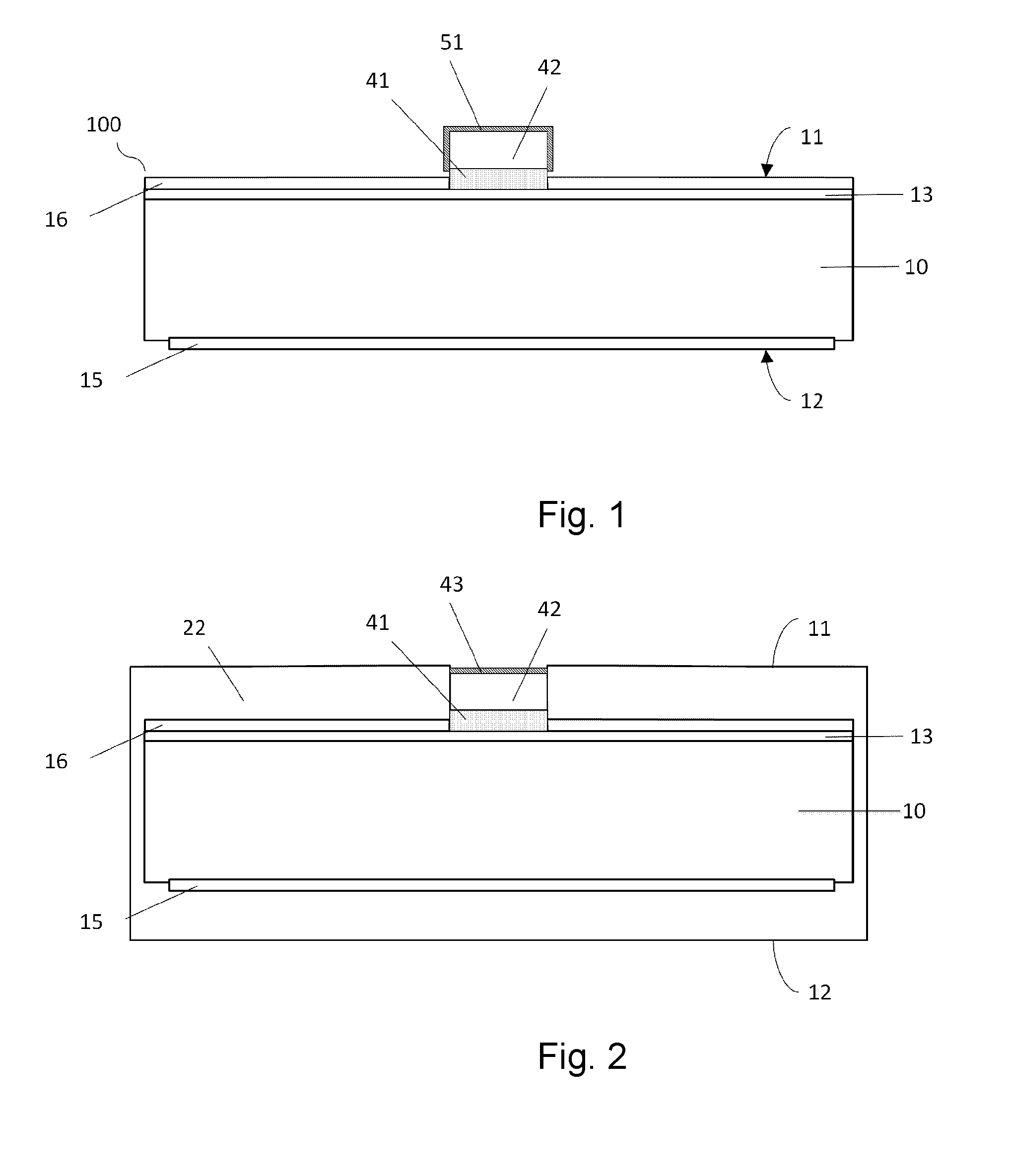
[0053]Thereafter, a protective layer of an insulating silicon compound is formed. This is most suitably a native silicon oxide. This is suitably achieved by removal from the substrate out of the deposition chamber, or alternatively, the introduction of air into the deposition chamber. The native silicon oxide typically has a thickness in the order of 2-3 nm, for which it consumes partially any underlying excess and / or copper silicide. FIG. 2 shows a diagrammatical cross-sectional view of the invention. In this embodiment, a front side 11 and the rear side 12 are covered with an insulating mask 22a, into which a cavity is present. This cavity is filled with the interface layer (41), the copper containing conductor (42). The insulating mask 22a effectively defines an exposed surface of the conductor (42), in the sense of limiting the surface that can be exposed by means of reduction of any native copper oxide. Thereafter, this surface is exposed, for instance by atomic hydrogen in a p...

third embodiment

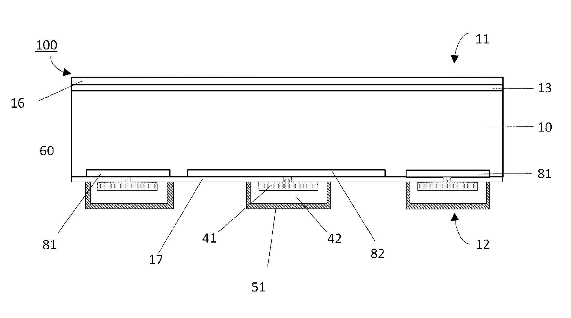
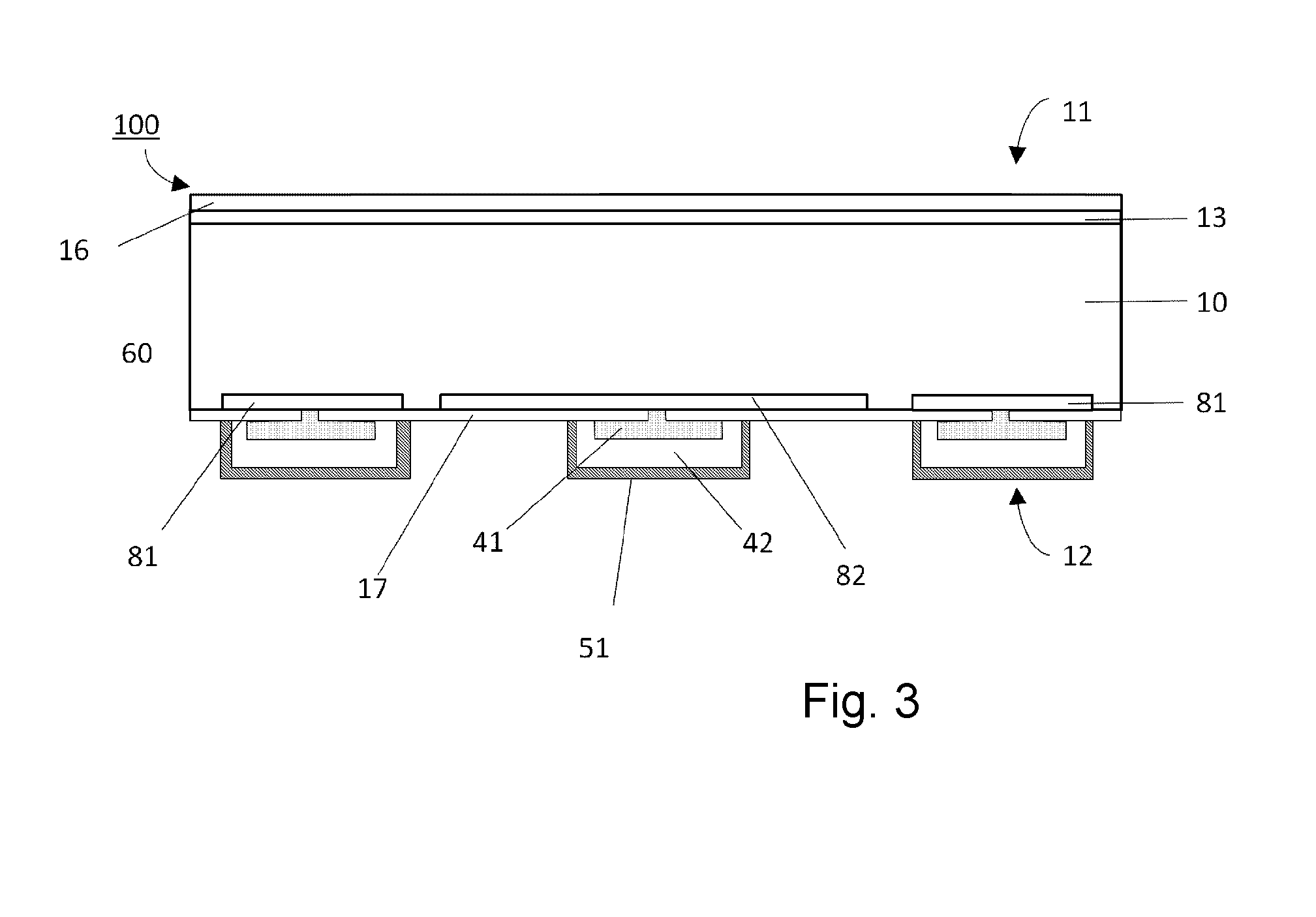
[0055]FIG. 3 shows a diagrammatical cross-sectional view of the invention. The shows device is again a solar cell, in this embodiment in an interdigitated back contact cell (IBC) design. A substrate 10 is provided with a front side 11 and a back side 12 having a front surface field 13 that may be textured and is covered with a passivation layer 16 that also serves as an anti-reflective coating. The back side has the emitter 82 and base 81 regions. In this case an n-type solar cell is concerned, which results in boron doped, p+ regions which form the emitter 82 and phosphorus doped n+ regions creating the base contact 81. Metal is contacting the emitter and base regions through small openings 60 of the back side passivation 17. The interface layer 41 is built up of a stack of metals, aluminium, tungsten-titanium stack. This stack provides good contact to the emitter and base regions and also serves as a barrier layer for the copper conductors 42. The copper conductor is covered by th...


PUM

PropertyMeasurementUnit
temperatureaaaaaaaaaa
thicknessaaaaaaaaaa

Abstract

The method of manufacturing a solar cell comprises the steps of: (a) providing the semiconductor substrate in a deposition chamber of a vapour deposition apparatus, which semiconductor substrate comprises a passivation layer at a first side thereof which passivation layer is patterned to define contact areas at which the copper-containing conductor is present; (b) supplying a gaseous silicon species into the deposition chamber, resulting in the formation of a surface layer of a copper silicide on a surface of the copper-containing conductor and in the formation of amorphous silicon on top of the passivation layer, and (c) providing a protective layer of an insulating silicon compound on the surface layer, wherein the protective cover comprising both the surface layer and the protective layer.

Description

FIELD OF THE INVENTION[0001]The invention relates to a method of manufacturing a solar cell with a copper-containing conductor covered with a protective cover, comprising the steps of: depositing the copper-containing conductor on a substrate, and providing the protective cover on an exposed surface of the conductor.[0002]The invention further relates to an electronic device thus obtainable.BACKGROUND OF THE INVENTION[0003]Solar cells need conductors for electrical connection of electrodes in the substrate to terminals. Typically, the electrodes are defined as highly doped regions in the semiconductor substrate. After passivation of the semiconductor substrate, such passivation layer is locally opened and a conductor is applied locally.[0004]Generally, two methods of conductor deposition on solar cells are available: the use of a screen printed metal paste and the use of electroplating, particularly with copper. A metal paste has a composition for local removal of any underlying ins...

Claims


Application Information

Patent Timeline
Patent Type & Authority Applications(United States)
IPC IPC(8): H01L31/0224H01L31/048H01L31/0216H01L31/18
CPCH01L31/022425H01L31/02167H01L31/048H01L31/18Y02E10/50
Inventor WOLTERS, ROBERTUS ADRIANUS MARIALUCHIES, JOHANNES REINDER MARCHERES, KLAAS
Owner M4SI
Why Eureka
Try Eureka